Chapter 2 -
Thinking Inside the Box
Reverse engineering can be thought of as a very challenging yet very rewarding game. To win, you need a bit of skill and a bit of luck. And like any game, to develop your skills you just need to play, play, play.
The first step in building your skills as a hacker is to develop an intuition for the material. In the case of hardware, a good way to get a feel for things is to take the covers off of everything and try to figure out what all the components are, and what they might do. It is also helpful to order a paper catalog from a parts vendor such as Digi-Key, Jameco or Newark Electronics and just leaf through the pages in your spare time. At first, reading through a parts catalog may feel like reading a dictionary, but as you look at more and more circuit boards, you will gradually find that everything makes sense.
The next most powerful tool of the reverse engineer is pattern matching. All hardware engineers are constrained by the same laws of nature, and all hardware engineers use the same kinds of building blocks. Engineers also like to modularize and reuse existing designs. As a result, a single design motif can be found in many designs. Recognizing design motifs will enable you to determine the function of circuits even if you do not recognize a single part number. Likewise, one can go quite far in reverse engineering without any formal electrical engineering training.
The final tool of the reverse engineer is experimentation. When intuition and pattern matching fail to reveal the secrets of a circuit, one must resort to probing and perturbing the system and trying to deduce function based on the observed responses. While experimentation may lead to hardware failure, one can take solace in the fact that most consumer hardware is designed to be probed and tested as a requirement for manufacturing. Furthermore, in the case of the Xbox, one can take some comfort in the fact that a new Xbox is relatively inexpensive. Buying two boxes up front and treating one as the “sacrificial” box helps remove the psychologicalbarrier one might otherwise have about performing aggressive experiments on the hardware.
This chapter will introduce you to the basics of reverse engineering, with a focus on basic techniques, such as reading circuit boards to build an intuition, and some coverage of intermediate techniques such as pattern matching and recognizing basic design motifs.
Reading a Circuit Board
The first thing you see when you take the cover off of a typical electronic device is the circuit board. Typically colored green or tan, this multilayer sandwich of copper, glass fiber and epoxy contains an exact schematic netlist within its traces. In other words, by following the traces, one can determine exactly how every component is connected. The placement of components and the layout of the traces also contains clues that can bring insight into the designer’s thought process.
Circuit Board Basics
A typical circuit board consists of a few layers of patterned copper separated by thin sheets of fiberglass impregnated with epoxy. The color of a raw circuit board is whitish or tan with copper traces; however, almost all circuit boards are coated with a thin polymer called the soldermaskthat gives circuit boards their familiar green color. Molten solder does not adhere to the soldermask, so during production excess solder does not stick to the board and cause shorts. The soldermask has openings for connections to components. These openings typically have a silvery color from a thin plating of tin or solder that is applied to prevent the copper from oxidizing and to enhance solderability.
On top of the soldermask is typically a layer of white lettering referred to as the silkscreen. Each component on a circuit board has an outline and a unique designator on the silkscreen layer. The designator enables people to quickly associate a component on a circuit board with a component on a schematic. You can use the designator to help guess the function of acomponent based on the component naming scheme. Table 2-1 summarizes the component naming scheme used in the Xbox.
Tip
 The Xbox motherboard includes a handy coordinate system printed along the edges of the board in the silkscreen layer. On the component side of the board, the coordinates go from A through G on the sides, and from 1 through 8 along the top and bottom. The reverse side of the board has coordinates M through V along the sides. Note that theletters I, O, Q, and S are skipped because they can be confused with the numbers 0, 1, and 5. Component designators on the Xbox motherboard are encoded using this coordinate system; thus, J7D1, the LPC debug port, can be found on the top side at coordinates 7D. This book will frequently use this coordinate system along with the component designators to refer to specific components.
 Connections between wiring layers are made by copper-filled holes called vias. Since the cost of a circuit board grows with the number of layers, most consumer electronic devices are designed to keep the number of layers to a minimum. Radio receivers and audio amplifiers will typically use single-sided boards, whereas the latest PC motherboards might have up to six oreight layers. The Xbox motherboard has four layers. The top two layers are dedicated to carrying information between chips, and the inner two layers are dedicated to delivering power. The Xbox motherboard will appear opaque at first glance because the inner power layers are basically solid sheets of copper. The good news for reverse engineering is that we can trace every connection on the Xbox motherboard through casual visual inspection because all of the signals layers are outside of the opaque power layers. The Xbox design contrasts with motherboards that bury two or four signal layers inside of the power layers. Buried signal layers can make signal tracing difficult. (Note that the decision to bury signals inside powerlayers is typically not driven by security, but rather by the physics of how electrical signals interact between circuit board layers.)
| Designator | Component Type |
|---|---|
| C | Capacitor |
| R | Resistor |
| U | Integrated Circuit or Transistor |
| L | Inductor |
| RP | Resistor Pack |
| Q | Transistor |
| CR | Diode |
| J | Connector or Jumper |
| RT | Resettable Fuse |
| Y | Crystal |
Table 2-1: The Xbox component naming scheme.
It’s fairly easy to trace a signal. Starting from the connection of the source component to the board, follow the copper trace. If the trace intersects with a circle, then there is a good chance that the signal continues on the opposite side of the board. If a trace ends and there is no connection to the other side of the board, there is a good chance that the trace is connected to one of the power planes.
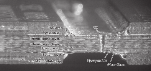
Figure 2-1: Cross-section of a typical circuit board.
Try it

Try tracing some signals on the Xbox motherboard. On the Xbox motherboard, take a look at connector J8C1, the 40- pin IDE connector in sector 8C. Almost all of the signals from the IDE connector go to one chip, the MCPX, on the motherboard by way of some resistor packs. What might you be able to conclude about that chip? Notice how some of the traces coming from the IDE connector mean der back and forth. This is a technique used to try and ensure that all wires have the same length. See the sidebar on “Why do Circuit Board Traces Meander Everywhere?” for more explanation.
Components
Now that you have a little bit of experience tracing back a signal, it is time to learn what some basic components look like. Components are classified as passive and active. Loosely speaking, passive components cannot amplify a signal, so they usually have just two leads. Sometimes multiple passive components are packaged together, so a single package of passive components will have multiple leads. Passive components include capacitors, resistors and inductors. The most common passive components on the Xbox motherboard are capacitors. Capacitors store energy as an electric charge; in the Xbox, they are primarily used to smooth out local power fluctuations from CMOS digital logic switching, and to suppress high frequency noise.
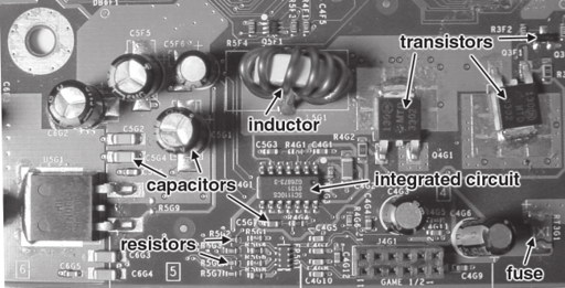
Figure 2-2: Typical passive components in an Xbox.
Why Do Circuit Board Traces Meander Everywhere?
After looking at a few circuit boards, you will probably start noticing that the traces on the circuit board often times meander all over the place, sometimes going back andforth several times before connecting to their destination. This seems pointless when a straight trace would do the trick. However, rarely will you find a structure on a circuitboard that was placed as a flighty whim by the designer. It turns out that the speed of signals in most high-end electronic devices, about ¼ the speed of light, is slow compared to the time required for a signal to arrive at its destination. For example, a signal will only travel 3 inches on a circuit board during one clock cycle in a 1 GHz processor (one clock tick at 1 GHz is a duration of 1 billionth of a second, or one nanosecond). Thus, two signals starting from the same chip will arrive at their destination at quite different times if the trace lengths are very different. To combat this, designers will put extra bends into the shorter trace so that the effective length of the trace is the same as the longer one.
Other large passive components found on the Xbox motherboard include inductors and resistors. The large wire-wound toroidal (donut-shaped) inductors found on the Xbox motherboard are all part of the power supply subsystem. Inductors store energy as magnetic flux. An inductor’s electrical properties are complementary to that of a capacitor. Combinations of inductors and capacitors with transistor switches in between are used to build very efficient power regulators. Most of the resistors on the Xbox motherboard are used either to absorb excess energy at the termination of signal traces, or to bias a wire to a particular logic level.
There are two ways you can identify a passive device on the Xbox motherboard. The first is by the shape of the package. Package shape recognition is feasible because there are so few basic varieties of passive parts. Figure 2-2 has some pictures of the capacitors, inductors, andresistors that you might see on an Xbox motherboard. The second method is to read the label next to the part on the motherboard and to infer the part’s function by the reference designator, using Table 2-1 as a guide.
Active components can amplify signals, and have three or more leads. The simplest active component is a transistor, with three and occasionally four leads (sometimes discrete “MOSFET” transistors have an explicit fourth “body” terminal). The most complicated active components are integrated circuits, such as CPU and memory chips, with hundreds, sometimes thousands, of leads. Integrated circuits come in a wide variety of packages, and sometimes the connections are hidden underneath the package, as is the case in the Ball Grid Array (BGA) package. The graphics chip, MCPX, and CPU on the Xbox motherboard use BGApackages. Figure 2-3 shows a cross section of a BGA device, revealing the hidden connections underneath.
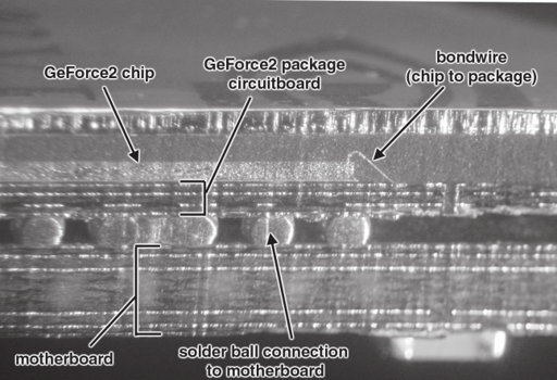
Figure 2-3: Cross sectional view of a BGA packaged part (GeForce2) mounted on a motherboard.
What Are All These Resistors and Capacitors Doing on a Digital Circuit Board?
A motif you will notice on many circuit boards is a preponderance of resistors and capacitors. Capacitors are everywhere because they help keep noise to a minimum andstabilize the power supply voltages. They are required because the copper planes used to distribute power have a small amount of resistance and inductance. These smallparasitics can cause big problems when a large amount of current is switched through the power supply. The exact placement and selection of capacitors is considered a bit of a black art. If you happen to knock off one of the tiny, sand-grain sized capacitors on a circuit board while working on it, chances are that you’ll be able to get away without replacing it. However, given a defect of this kind, the most likely problem you will encounter are intermittent reliability problems.
While capacitors are everywhere to provide local storage of energy for all the components, the resistors remove excess energy. Fast signals on a motherboard carry a lot of energy, and if the energy is not dissipated at the receiver in a controlled fashion with a resistor, the signal energy will reflect back to the transmitter and cause problems. The phenomenon is similar to that of sound in a gymnasium. When you speak in an empty gymnasium, there is an echo. If you speak too fast, people will be unable to understand you because the echo will start interfering with your speech. However, if you cover the gymnasium walls with foam, the echo will be absorbed by the foam and you can talk without interference from your echo.
Resistors are like the acoustic foam you would put on walls to damp out echoes, so that circuits can talk to each other at high speeds. Unlike most capacitors, if you happen toknock off one of these resistors while playing around, you will have to replace it in order for the circuit to work properly. These “termination resistors” are often packaged four oreight to a package, so they almost look like small integrated circuits. You can distinguish resistor packs from other components because they are shiny, slightly lumpy, have a white border, and they will have a reference designator prefix of “RP” near them. When tracing a signal through a resistor pack, it is fairly safe to assume that signals flow straight through, so that a connection on one side goes straight through to the pin immediately on the other side.
Identifying the function of a particular integrated circuit is more challenging than identifying the function of a passive device. Functionally identical silicon can be purchased in a variety of packages that can look very different. In some cases, you can guess the function of a device by observing what the device is connected to or what it looks like, but the most reliable method is to read the part number off the chip and look it up on the web. (Typically, parts have some kind of logo or part number prefix that identifies the manufacturer, which you can use to find more data on the device by visiting the manufacturer’s website.) If you do not recognize the logo or the part number prefix, the services listed below can help you look up part functions.
1. www.findchips.com can take a part number or pieces of a part number and search the inventories of many distributors for inventory matches. Most common parts will show up inFindChips, and the links provided will often lead you not only to a short description of the part, but also pricing and ordering information.
2. www.google.com indexes everything on the web, and part numbers are no exception. Google can also be used to help find manufacturer’s websites if you query on the letters in the logo plus a descriptive term such as “semiconductors.” At the manufacturer’s website, you will probably need to find the specialized part search engine buried in the website or go to the semiconductor products sub-page in order to do a part number lookup. The search function on the front page of a company’s website will sometimes find part numbers, but more often it indexes only useless corporate and marketing pages.
3. If neither of these services gets you there, try stripping off some of the prefixes and suffixes on the part number. In our M29F080A example, querying just the part number 29F080 willbring you to the webpages of multiple manufacturers who make parts that are functionally compatible with the STMicroelectronics part.
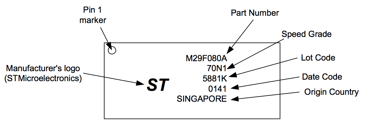
Figure 2-4: Anatomy of a typical IC part number. The diagram is a cartoon of the chip at location U7D1 on the Xbox motherboard.
Try It

Let’s try looking up an Xbox part number. Locate U7D1 on the Xbox motherboard. Figure 2-4 illustrates what you might find. The part number is typically the longest number on the chip, and it often starts with one or two alphabetic characters. Memory chips and processors also frequently have a speed grade or quality suffix after the part number. Additionally, almost all chips have adate code. Date codes are usually a four digit number of the format YY-WW, where YY is the year the chip was manufactured, and WW is the workweek. In our example, our M29F080A part was manufactured in the 41st week of 2001 in Singapore, and it has a speed grade of 70N1. The remaining number, 5881K, is a lot code whose meaning varies between manufacturers, but in general links a chip to a particular silicon wafer or silicon wafer lot’s tracking number in the fabrication facility.
The “ST” logo indicates the manufacturer of this chip is STMicroelectronics, and fortunately the website for this manufacturer can be quickly found through Google or byguessing, as the URL for the company is simply www.st.com. Entering the part number M29F080A into the search field on the home page brings you directly to search results that include detailed datasheets and descriptions of this part — an 8 Mbit Uniform Block Single Supply FLASH ROM.
Test Points
Almost all circuit boards in consumer electronics feature structures designed to expedite the testing of the finished board in the factory. These “test points” exist to cope with the unfortunate reality of manufacturing defects. The Xbox is no exception when it comes to test points and manufacturing defects. The bottom of the Xbox motherboard is populated with hundreds of test points — tiny silvery circles — that allow a contact probe to access almost every interesting signal within the Xbox. These test points are a welcome gift to reverse engineers and to people who wish to modify their hardware, because they provide easy access to signals that might otherwise require a microscope and a steady hand.
A set of test points are probed all at once on the manufacturing line with a piece of equipment called a “bed of nails tester.” Aptly named, the bed of nails tester consists of hundreds of spring-loaded “pogo pin” structures. A motherboard is aligned to the testbed and clamped down with either mechanical plungers or a vacuum chuck. Similarly, you can use pogo-pins to make your own solderless modifications to an Xbox motherboard by leveraging the test points. You wil need to build your own circuit boards (see Appendix), but the result will be a board that you can install simply by screwing it down — no soldering required!
Xbox Architecture
Before diving into the pattern matching examples, we will need a pattern reference. Let’s take this opportunity to study the Xbox internal architecture as the pattern reference, and eventually compare the Xbox architecture to a PC and to another video game console.
High-Level Organization
The Xbox has a Pentium-III class processor running at 733 MHz as its CPU. The “S-Spec” number on the CPU is closest to that of a Mobile Celeron. The CPU is connected via a standard P6 133 MHz Front Side Bus (FSB) to a graphics processing unit (GPU) and a northbridge combo chip called the NV2A by nVidia. Its closest PC relative is the nForce IGPchip by nVidia. Since the northbridge logic and the GPU are combined in a single chip, the CPU and graphics processors can share a common bank of memory. This is cal ed a “unified memory architecture” (UMA). Compared to a traditional split video/main memory architecture, a UMA costs less to build because it eliminates the dedicated video memory. However, UMA has lower performance in certain situations because it introduces memory access contention between the main processor and the graphics processor. In order to alleviate some of thiscontention, the system memory is frequently split into multiple banks. The nForce IGP, for example, splits the memory into two banks that can be independently accessed by both the GPU and the CPU through a switching network.
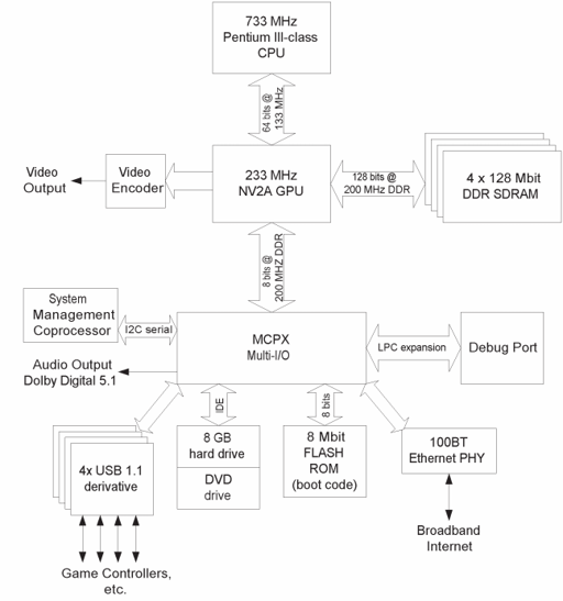
Figure 2-5: High level architectural view of the Xbox.
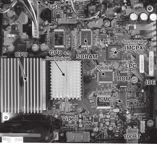
Figure 2-6: Photograph of an Xbox motherboard with the major components labelled.
The GPU is connected to a kitchen-sink chip called the “MCPX” via a fast, narrow bus called a HyperTransport bus. The MCPX combines a southbridge chip plus almost all of the Xbox peripherals, including USB controllers, a legacy boot ROM interface, a Dolby digital audio processor, a mass storage IDE controller, an ethernet control er, and interfaces to system management functions.
The connectivity of all the major blocks in an Xbox are illustrated in Figure 2-5, and Figure 2-6 illustrates the location of these blocks on an actual Xbox motherboard.
Functional Details
The following sections present a cursory overview of the pieces that constitute the Xbox architecture. We pay particular attention to the details necessary for understanding how to reverse engineer the Xbox security mechanisms.
CPU
The CPU (Central Processing Unit) is the computational heart of a conventional computer. The subject of CPU architecture deserves an entire book alone, so we will cover just the material required to understand how to reverse engineer the Xbox. In particular, we will investigate how to gain control of the Xbox CPU.
A CPU reads sequences of instructions stored in memory — programs — that tell the CPU to perform various computations or to make decisions based on available data. The instructions are stored in memory as numbers called opcodes. Opcodes take operands as arguments. Programmers use alphabetic mnemonics when writing low-level machine code so that they don’t have to remember hundreds of opcode numbers. For example, a kind of byte-wide subtraction instruction has the opcode 0010.1000 (binary) or 0x28 (hexadecimal) and the mnemonic “SUB”. The requisite subtraction opcode varies depending upon the source andwidth of the subtraction data. Keeping track of all of the opcode to operand rules is overwhelming, so the process of translating mnemonics and operands to instruction numbers is accomplished with a program called an assembler. Likewise, the process of translating instruction numbers back into mnemonics is done with a disassembler. Significantly, most programs are not written in assembly language; a higher-level language, such as C, is typically employed. These high-level languages are translated into machine instructions using compilers. Automatic decompilation of machine instructions back into a high-level languagecan be difficult because the process of compilation — especially optimized compilation — discards much of the high-level structural information contained in the original source code.
The processor keeps track of which instruction is being executed with an instruction pointer(IP). An IP is also referred to as a program counter (PC) in some contexts. IPs typically advance through a program one instruction at a time, unless a branch instruction is encountered. A branch instruction gives the program an opportunity to make a decision by inspecting data inside the CPU and jumping to a new location based on the outcome of the inspection. Understanding the movement of the instruction pointer is a central part of reverse engineering an Xbox. Being able to manipulate the IP is tantamount to having control of what the Xbox can and cannot do. The security measures implemented in the Xbox software architecture attempt to guarantee that the IP is always executing only Microsoft-approved codeby always cryptographically verifying a piece of code for authenticity before running it.
Binary and Hexadecimal Numbers
Digital circuits use 1’s and 0’s to represent numbers. This binary, or “base-2”, notation is a reflection of the way electrical signals are used to represent numbers: two ranges of voltage levels are used to define one logic state or the other. It is possible to build electrical systems that represent information using more than two voltage levels, but only at the cost of power and complexity. Modern modems, for example, use multiple voltage levels and phase information to represent multiple bits of data in a single time unit.
Number composition and arithmetic in binary follows the same rules as our familiar decimal (“base-10”) representation. In decimal, 0’s are used as placeholders to remember when a digit has overflowed. For example, 1 more than 9 leads to an overflow because there is no single digit bigger than 9. Hence, the number 10 recordsthat we had one overflow of the right-most decimal location. Likewise, in binary, 1 more than 1 is 10, since the largest single digit in binary is 1.
Thus, in decimal, the value of a four-digit decimal number d4d3d2d1 can be broken down as:
d4 * 103 + d3 * 102 + d2 * 101 + d1 * 100 = d4 * 1000 + d3 * 100 + d2 * 10 + d1 * 1
Likewise, a four-digit binary number b4b3b 2b1 can be broken down as:
b4 * 23 + b3 * 22 + b2 * 21 + b1 * 20 = b4 * 8 + b3 * 4 + b2 * 2 + b1 * 1
For example, the number 1010 = 1*8 + 0*4 + 1*2 + 0*1 = 10 decimal.
Keeping track of numbers in straight binary can become cumbersome quickly; for example, to represent decimal 968, you need ten binary digits. To save on screen space, binary numbers are converted to octal or hexadecimal. The octal format, or “base-8”, was popular in the early days of computers, but has since become a rarity. Hexadecimal, or “base-16”, is the de-facto numbering system. There are 16 digits in hexadecimal, so the hex digits that correspond to decimal numbers 10 through 15 are represented by the letters A through F. Table 2-2 summarizes the conversion betweenbinary, decimal, and hexadecimal for the first 16 positive integers.
In order to differentiate hexadecimal from decimal numbers, many people use the C language convention where 0x[number] represents a hexadecimal number, and [number] is implicitly a decimal number. Binary numbers have no similar standard to draw from in C, so some people use the Verilog standard, [digits]’b[number], where [digits] is the number of digits in the binary number. The suffix “b” after a string of 1’s and 0’s, such as 1010.1100.1110b is also used to denote a binary number. Notice how a “.” was used to group the binary digits into sets of four; this assists in mentally translating the binary number into hexadecimal: 0xACE.
| Bin | Dec | Hex | Bin | Dec | Hex | |
|---|---|---|---|---|---|---|
| 0000 | 0 | 0 | 1000 | 8 | 8 | |
| 0001 | 1 | 1 | 1001 | 9 | 9 | |
| 0010 | 2 | 2 | 1010 | 10 | A | |
| 0011 | 3 | 3 | 1011 | 11 | B | |
| 0100 | 4 | 4 | 1100 | 12 | C | |
| 0101 | 5 | 5 | 1101 | 13 | D | |
| 0110 | 6 | 6 | 1110 | 14 | E | |
| 0111 | 7 | 7 | 1111 | 15 | F |
Table 2-2: Binary, decimal, and hexadecimal conversion table.
The heart of a CPU is a tiny, but very fast, memory called the register file. Multiple pieces of data can be written into and read out of a register file each processor clock cycle. Data from the register file is fed into an execution unit called the arithmetic logic unit (ALU). The functioncomputed by the ALU is controlled by instructions fetched from memory. Once the data has been processed by the ALU, it can either be written back into the register file, or stored into memory.
One important performance feature of almost every modern CPU is a memory access accelerator called a cache. Caches are small, fast memories that store copies of data and instruction snippets that are likely to be used in the near future by the CPU core. Caches are slower than register files but faster than main memory; likewise, caches store more data than aregister file, but store less data than main memory.
One important feature of the Xbox CPU cache to be aware of is that it is a writeback cache. Writeback caches allow copies of data stored inside the CPU to be out of sync with what exists in main memory. This timing difference can complicate attempts to trace CPU execution by observing external memory traffic alone. The cache memory can also be leveraged by security routines to hide intermediate computation results from someone observing the memory bus.
Northbridges and Southbridges
The terms Northbridge and Southbridge are vernacular specific to the PC architecture. They refer to the two basic support chips that are found in virtually every PC. A Northbridge chip connects the CPU to main memory as well as any high-performance expansion busses, such as AGP and PCI. A Southbridge chip hangs off of the Northbridge chip and contains all of the extra peripherals that are found in a typical PC — parallel, serial, USB, mouse, keyboard, IDE controllers, audio codecs, and more. Dividing the PC architecture into these three main modules — CPU, Northbridge and Southbridge — enables PC designers to mix and match different kinds of memory architectures with a diverse selection of processors and peripherals.
The connection between the Northbridge and the Southbridge chipsets varies from chipset to chipset. In the case of the Xbox, a high performance, narrow parallel bus called HyperTransport is employed as the connection between the functional equivalent of the Northbridge and Southbridge chips. The bus is only 8 bits wide in each of two directions, but it is clocked at 200 MHz and data is sampled on each clock edge so the effective peak transfer rate is 400 Mbytes/second in each direction. A Northbridge chip is connected to a CPU via a bus called the Front Side Bus (FSB). In the case of the Xbox, the FSB is a 64-bit 133 MHz bus that uses AGTL+ logic levels.
Knowing and understanding the kinds of connections between chips is crucial in reverse engineering because the kind of connection will dictate how difficult it is to intercept data going between various components. The details of the relatively easier bus to tap, the HyperTransport bus, are discussed in Chapter 8, “Reverse Engineering Xbox Security.”
In the Xbox, the Southbridge is a chip designed by nVidia called the MCPX; it is a derivative of the nVidia nForce MCP Multimedia and Communications Processor. The Northbridge chip was also designed by nVidia, and it is called the NV2A GPU. Both the Northbridge and Southbridge chips were manufactured by TSMC (Taiwan Semiconductor Manufacturing Corporation). The NV2A combines both a GPU (Graphics Processing Unit) and the traditional memory and expansion bus controllers found in most Northbridge chips. As explained previously, combining the graphics processor and the Northbridge allows system designers to merge the graphics memory into main memory, at some performance penalty.
RAM
The Xbox motherboard employs 64 MB of DDR SDRAM for the main memory. DDR SDRAM stands for Double Data-Rate Synchronous Dynamic Random Access Memory. By combining synchronization and DDR techniques, the aggregate bandwidth of the Xbox main memoryachieves 6.4 Gigabytes/second. A RAM is basically a table of information that is indexed by the CPU. Each location in RAM has a unique index number called its address, and as the name “random access” implies, there are no restrictions on the order of data access in a RAM.1
The term “dynamic” is applied to RAM that has to be constantly refreshed in order to preserve the integrity of data. For example, the RAM used in the Xbox must have every location read out and written back about thirty times a second. The performance penalty is not as bad as it sounds, as special hardware is built into modern DRAM chips that help optimize the process.
The “synchronous” prefix means that inside the DRAM, the procedure for data access is broken down into a series of steps. Each of these steps are independent and can occur in parallel, so that multiple data requests can be in-flight simultaneously. An external timing signal, known as a clock, is used to synchronize the movement of data access requeststhrough the various steps inside the DRAM. As a result, data access requests flow through each step like water through a pipe, and this technique is also known as pipelining. Synchronous DRAMs have higher bandwidth throughput than their predecessors, because pipelining allows multiple requests to be processed at once. However, the time required from when an access is first issued to an SDRAM to when the data finally appears on the output —the access latency — is not improved by pipelining.
The term “Double Data Rate” refers to the way synchronous data is transferred relative to the synchronizing clock. A clock waveform consists of a repeating pattern of high and low signals. In traditional systems, data is only transferred on the low-to-high transition of a clock waveform. In a DDR system, data is transferred on both the low-to-high and the high-to-low transitions. Thus, for the same clock frequency, twice the amount of data can be transferred. The performance mnemonic quoted by DDR SDRAM vendors, such as DDR266, refers to thetransfer rate, so the actual clock speed is one-half the performance mnemonic, or 133 MHz in this case.
ROM
Every computer needs to have some kind of persistent or non-volatile memory for storing the start-up, or boot, program. The DDR SDRAM discussed above does not work for this application because all data in a DDR SDRAM is lost when the power is removed. Current versions of the Xbox use a FLASH ROM instead to store data that has to persist even when the power is turned off. ROM stands for Read-Only Memory, and FLASH refers to a specific style of storage element that is electronically reprogrammable. FLASH style memories are convenient in PCs because they can be reprogrammed by the end user to fix mistakes in theboot code. However, in the Xbox, FLASH ROM programming by the end user is purposely disabled. The write signal required for programming is disconnected by leaving out the jumper located on the back of the Xbox motherboard at component location R7R4 (see the sidebartitled “Enabling FLASH ROM Programming Hardware” for more information). In the case of the Xbox, the reprogrammability of FLASH is primarily leveraged as a convenience for Microsoft during development and production. It is quite likely that in a few months, the Xbox will use cheaper hard-wired “mask ROMs” once Microsoft believes it is ready to etch its boot program and kernel in stone (or silicon, as the case may be).
The boot ROM is pivotal in reverse engineering any computer because it contains critical code that is responsible for initializing the whole system. In the case of the Xbox, the boot FLASH ROM plays an even more crucial role because it is partially responsible for implementing the tight software security system. The exact role of the FLASH ROM in the security system will be explained later, but the important thing to remember for now is that the FLASH ROM controls the initialization of the hardware in the Xbox and also contains the initial operating systemkernel image.
Enabling FLASH ROM Programming Hardware
Patching the signal that was disconnected by Microsoft in order to prevent in-system FLASH ROM programming is a fairly simple procedure. The FLASH ROM write signal was disconnected by omitting a single resistor, component number R7R4, located on the bottom side of the Xbox motherboard at sector 7R. You can solder a piece of wirebetween the two silver pads of the resistor, or you could even simply bridge the pads with a large amount of solder. Note, even though FLASH ROM programming is enabled in the hardware by this patch, you still do not have a program that actually does the reprogramming. Running sucha program is a much greater challenge due to the cryptographic software security system put in place by Microsoft.
Odds and Ends
The Xbox features a small 8-bit coprocessor called the System Management Controller (SMC). The SMC is a complete miniature computer with RAM, ROM, and a processor in a single package. The processor inside the SMC uses the PIC (Peripheral Interface Controller) architecture, originally developed at Harvard university around 1975 and adapted by General Instruments for commercial sale. Arizona Microchip Technology (now called Microchip Technology, www.microchip.com) acquired the PIC product line in 1985 and has been selling it ever since. The SMC can be found in sector 7B on the Xbox, and its reference designator is U7B2. The SMC monitors the power button on the front of the Xbox, so the SMC must run even when the CPU is turned off. As a result, the Xbox power supply has a low-current 3.3V “standby” power line that is always active when the Xbox is plugged in. The SMC is also responsible for controlling the lights around the power button on the Xbox, and it controls the DVD eject mechanism as wel . Final y, the SMC has a function that monitors the health of the CPU, and reboots the CPU in case it crashes. The SMC monitoring function must be disabled if youwish to run your own operating system on the Xbox. The SMC talks to the CPU via the MCPX through a 1-bit serial interface known as I2C.
Another important feature of the Xbox is the LPC debug port. The LPC debug port is a 4-bit wide bus that runs at 33 MHz. LPC stands for “Low Pin Count,” and it was originally devised as a method for connecting a large number of slow legacy devices, such as keyboards, serial ports, parallel ports and boot ROMs, to the Southbridge chip via a simple intermediate translation chip. The debug port is provided on the Xbox presumably for manufacturing test purposes by Microsoft’s hardware contractor. When the Xbox nears its final stages in production, the LPC debug port is used to load a boot program that performs tests, diagnostics and burn-in on the Xbox motherboard. The LPC debug port is discussed in more detail in chapter 11, but the important thing to know for now is that one can force the Xbox to read its initial boot ROM image through the LPC debug port by connecting an LPC-compliant ROM device and shorting one of the data pins (D0) on the FLASH ROM to particular voltage (zero volts). This is perhaps the easiest method for forcing the Xbox to boot your own code — given that you know how to get around the secret boot code that secures the Xbox.
Pattern Matching
Now that we are familiar with the Xbox architecture, we have a reference point for perhaps one of the most powerful reverse engineering tools — pattern matching. Being able to make educated guesses about the function of various parts by simply observing their connectivity, placement and shape is the first step in becoming a crack reverse engineer. To demonstrate the power of pattern matching, we will compare the Xbox motherboard to a PC motherboard and to a Nintendo Gamecube motherboard.
Learning a lot of patterns is the best way of becoming a good pattern matcher. I take apart every piece of equipment that I buy, and I pore over the circuit boards to try and learn what other designers know by “reading” the circuit board. Every circuit board tells a story about its design process; rarely will one encounter a peculiar circuit feature that does not have some intended purpose.
Caution

When taking apart any piece of electronic equipment, be sure to first unplug it and wait a minute for the charge on the large capacitors in the power supply to dissipate. Also be sure to use appropriate static electricity control measures described in chapter 1!
Comparison: Xbox Versus the PC
The similarity of an Xbox to a PC is a boon to hackers, since the PC platform is very wel documented. Every part in an Xbox has an analog in a typical PC, so almost any high-level question can be answered by just reading about a similar PC part. Thus, it pays to take a closer look at the similarities between the Xbox motherboard and a standard PC motherboard. Another benefit is that much of the information in this book will apply directly to PCs, so you can easily apply what you will learn from hacking the Xbox to a large number of situations.
The Xbox’s closest relatives are systems based on chipsets that use a unified memory architecture, such as nVidia’s nForce or Via Technology’s ProSavageDDR. The architectural diagram presented in the previous section was derived by reading the published specifications of the Xbox and material available on nVidia’s website about the nForce chipset. In this section, we will compare the Xbox to the Via Technology ProSavageDDR-based P4M266 motherboard. The Xbox is compared here with a non-nVidia chipset motherboard to emphasize the broad similarities of the Xbox to PCs.
Figure 2-7 shows a picture of a PC motherboard, the Via P4M266. Even though the chipset is manufactured by a different vendor, the similarities between the P4M266 and the Xbox are striking. Almost all of the material covered in the previous section applies to this PC motherboard. The primary differences are a few miscellaneous ports and connectors, and the presence of PCI and AGP high-performance expansion ports. The Via P4M266 also lacks an explicit LPC debug connector, since all of the legacy peripherals are directly realized by an LPC multi-I/O chip.
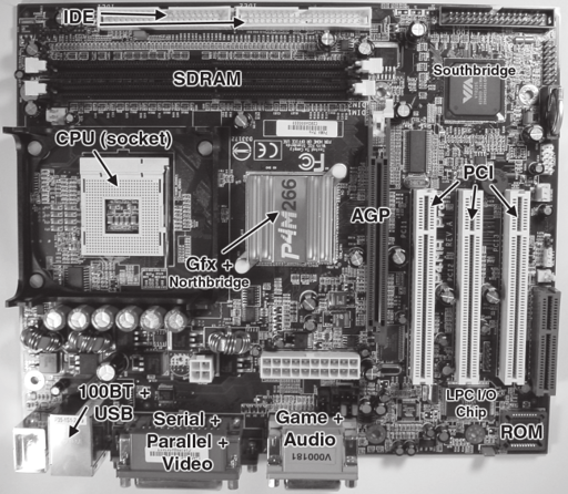
Figure 2-7: Via P4M266 motherboard with integrated graphics.
Contrast: Xbox Versus the Gamecube
The Nintendo Gamecube interesting in comparison with the Xbox. The Gamecube is a machine designed for the same purpose as the Xbox — gaming — but with a very different design philosophy in mind. The Xbox and the Gamecube both use the same gross architecture — a CPU, a graphics coprocessor, some memory, and some support chips — but the similarities end there. The Gamecube design demonstrates an exacting attention to detail and cost. The Gamecube motherboard is small and simple, the component count is kept to a minimum, and the heat sinking and thermal design is very simple. The clean, straight layout of most of the PCB traces on the Gamecube motherboard reflects the fact that almost every IC is custom-designed specifically for the Gamecube. As a result, the Gamecube is a much more economical platform to build than the Xbox.
One can recognize the gross organization of the Gamecube by inferring each chip’s function from the basic marketing information Nintendo provides. Further details about the architecture of the Gamecube are difficult to infer, because it uses so many custom components that have no counterpart in a standard PC. By the pattern of the traces on the motherboard, one would be lead to believe that the large chip in the center of the board, the “Flipper” chip, is the equivalent of an integrated graphics Northbridge chip in a PC. This is almost correct. A key difference is that even though the Flipper chip combines both a memory controller and a graphics controller into a single package, the graphics function still has its own dedicatedmemory, built inside the same chip. This kind of organization al ows a very high performance memory to be used by the graphics engine, with the trade-off of the memory being a bit smaller than if off-chip memories were used. The smaller size of the on-chip memory is compensated in part by the use of extremely fast off-chip memory.
The Gamecube does not use DDR SDRAM like the Xbox; instead, it uses what is cal ed a 1-T SRAM. 1-T SRAMs are DRAM memories that emulate a very fast type of memory known as the Static RAM (SRAM). SRAMs have much lower random access latencies than DRAMs, and they also do not require each memory cell to be refreshed 30 times a second like DRAM does. The actual magic behind how DRAM can masquerade as fast SRAM is fairly complicated and is beyond the scope of this book, but you can find more information at the 1-T SRAM manufacturer’s website, www.mosys.com.
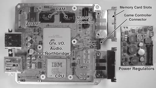
Figure 2-8: Gamecube motherboard plus its power regulator card. The motherboard is about half the size of the Xbox motherboard.
The Gamecube also has yet another piece of memory, known as ARAM, that is slower than the 1-T SRAM memory, and is used to store things like audio samples that do not require high-bandwidth accesses. Having a disparate memory architecture means that the Gamecube can squeeze a more consistent amount of performance out of each subsystem, something important in keeping frame lag to a minimum. The trade-off, however, is that the Gamecube can be more difficult to program, and mismanagement of the multiple pieces of memory can lead to performance problems.
Another important distinction between the Gamecube and the Xbox is that the Gamecube consumes much less power than an Xbox. Power consumption may seem unimportant at first, since both consoles are designed to be plugged into a wall outlet, but the Gamecube’s lowerpower envelope requires fewer heat transfer components and smaller power supplies to be used, saving on cost. Figure 2-8 includes a picture of the Gamecube power regulator for reference; the power regulator is a fraction of the volume of the Xbox power supply plus the local switching regulators on the Xbox motherboard.
To be fair, note that the Gamecube does have a small external AC to DC converter, while the Xbox takes wall power directly into the console. Furthermore, electronic components degrade much faster at elevated temperatures, as described by the rule of Arrhenius. For example, a 10degree Celsius operating temperature increase roughly doubles the failure rate of a component. As such, the Gamecube should be more reliable over the years than the Xbox since the Gamecube puts out less heat, and because its thermal management system is as good as, if not better, than the Xbox’s.
Finally, it is interesting to note that the Gamecube uses proprietary I/O interfaces everywhere. The game disk format is a mini-DVD format, and the DVD reader connects to the motherboard through a proprietary connector. Using a smaller DVD media allows Nintendo to reduce thelatency of data seeks, which means shorter game loading times. The game controllers and memory cards also use a proprietary signaling format. Everything in the Gamecube is somewhat similar to our familiar PC, but nothing was directly incorporated into the design unchanged.
In addition to optimizing the manufacturability and cost of the Gamecube, the use of mostly proprietary chips and standards makes the console much more difficult to reverse engineer than the Xbox. For example, note that in Figure 2-8, there is no obvious ROM chip in the Gamecube. Thus, in order to even start looking at Gamecube code, one has to hunt down and extract a ROM hidden somewhere in one of the chips on the motherboard! This is one of the rare times where security through obscurity works. Even if there were no security at all on the Gamecube, the cost and effort of trying to burn your own code onto Nintendo’s custom DVD format is just not worth it for the individual enthusiast.
1 Actually, SDRAMs can have a few restrictions on memory access patterns (such as page modes and burst modes) for performance reasons. The “random” moniker is intended to differentiate RAMs from First-In, First-Out (FIFO) and Last-In, First-Out (LIFO) style memories where data is accessed using a strict set of ordering rules.