Appendix E -
Debugging: Hints and Tips
Don’t Panic!
Developing your debugging skills is as important, if not more important, than developing your design skills. The most important single piece of advice is to never panic: randomly tweaking and changing things will introduce more uncertainty and bugs than it will fix.
Debugging is simple when given total visibility into a system and total knowledge of the expected state of a properly working system. Simply comparing the observed state against the expected state wil elucidate what went wrong. Unfortunately, the world rarely works this way. Chips are black boxes, and the only visibility into the internal state of the chip is through its pins. Many signals are also too difficult to directly measure or record. Also, the specifications provided by manufacturers are often vague or difficult to interpret. Thus, the real art of debugging is in tracing a set of symptoms to a root cause despite a lack of visibility and total system knowledge.
Understand the System
Trying to debug a system without first understanding what you are trying to debug is like trying to read a Japanese comic without any knowledge of Japanese. You can figure out at a superficial level who is the bad guy and who is the good guy, but you get really lost as to exactly what the floating cat has to do with all of it. In order to fully understand the plot, you need a Japanese dictionary and a lot of time and patience. Similarly, basic electronics principles and intuition will get you to the point where you know roughly what to expect, but enlightenment only comes after you have read the component data sheets. The more you understand about a system, the easier it wil be to figure out why things went wrong. Keep notes as you read more about the system, and think to yourself about ways problems might express themselves if something did go wrong. It also helps to have seen other systems that are similar to the one you are trying to fix, and it helps to have an understanding of the theory of operation.
Observe Symptoms
Bugs manifest themselves through symptoms, and it is up to you to deduce the root cause by observing several symptoms and deducing the culprit. A blank screen on a TV that should be showing the video output of your console is an example of a symptom. There are many reasons why your TV screen could be blank, such as a broken video cable, a broken TV, a broken video connector, a broken video source, blank media in the video source, or even lack of power to the system. As a general rule, you should observe at least two, preferably three, symptoms that are consistent with a cause before concluding that you have found the root cause. Keep in mind that the most telling symptoms are often not outwardly obvious, and will require a measurement or an experiment to find them. In the example of our blank TV screen, our measurements are as simple as seeing if the power light on the TV turns on, or if sound comes out of the TV without the video.
The basic strategy for debugging is to start with an obvious symptom and isolate various parts of the system to determine which part is the immediate cause of the symptom. An immediate cause is defined as something that directly impacts the observed symptom. Immediate causes for video failure on a TV are lack of a signal to the TV, a broken TV, or lack of power; non-immediate causes would be a hardware failure in your video source or the phase of the moon. In other words, given symptom A, think of all the possible immediate causes X, Y, and Z, and then test each to determine which is the actual cause. Once you have isolated the problem, think about what might have caused it to fail and repeat the process until you have discovered the root cause.
Isolating the cause of bugs can be facilitated by the use of known good references. In our example, you can eliminate the TV as a source of failure by feeding it a signal from a known good DVD player. In order for a known good reference experiment to be valid, you must keep everything constant except for the piece you are replacing with the reference. Plugging the good DVD player into a different input from the consoles’ on the TV will only tell us that the display part of the TV works. The path from the console input to the TV is not tested. A proper execution of the experiment would plug the DVD player into the video input used by the console.
This kind of paranoia or inherent mistrust of the system becomes very important when tracing down subtle hardware bugs. Do not take any factor for granted that could affect the system you are observing, and never, ever ignore an inexplicable or inconsistent behavior, even if it is intermittent. For example, sometimes a system will work properly or break if you touch a certain location on the circuit board or wave your hand near a certain area; sometimes a system will demonstrate different behavior for a brief moment after power-on. It is tempting to write off such observations as anomalies or trivial occurrences, but the fact is that they did happen and there must be an explanation. One specific example is touching a circuit board and observing a change in the state of the system. Where did you touch? How did you touch it? Are your hands sweaty or dry? When you touch a circuit board, your body acts like a small capacitance and a large resistance. This can slightly slow down signals or discharge high-impedance nodes such as an unconnected digital input. If you pressed firmly on the board, you could be flexing the board in such a way that changes the electrical properties of a cracked trace or a bad solder joint.
There are some symptoms that are often times incorrectly interpreted as causes. A burned-out trace or a damaged component is usually a symptom and not a cause of the problem. In other words, a malfunction elsewhere in the circuit is usually responsible for the failure of a component. Spontaneous component failure is a relatively rare occurrence. Suppose you are debugging a broken stereo. You smell something burning coming from the stereo, and you see a large resistor that is blackened from overheating. Chances are that if you just replace that resistor, the replacement will just burn out again. The real cause might be a shorted transistor or a damaged power supply circuit, but these do not manifest themselves as obviously as the burned out resistor.
Another potent observation technique is comparison against a known good system. If you are trying to debug a broken device, find a working one and compare voltages and other operational characteristics between the two. If you are trying to debug your own home-brew system, construct a simulation of the circuit if possible, or find a circuit with a similar design. You can use these known good systems to quickly isolate anomalous behavior. Furthermore, you can induce failures in the known good sample in a controlled fashion to check if you have really found the root cause of the problem. This technique is particularly applicable to simulated systems.
Common Bugs
The most common source of hardware bugs in home-brew projects are poor solder joints and improperly installed polarized components, such as capacitors, diodes, ICs, and connectors. Also, connectors are particularly notorious sources of failures because they are subjected to the most physical abuse and it is typically difficult to determine if a connector is in good condition through visual inspection alone. The following is a list of common bugs, ranked loosely in descending order of popularity.
- Bad solder joint. This includes cold solder joints, bridges, and forgotten joints. Careful visual inspection can catch many instances of bad joints. The solder between all joints should appear to be smooth and shiny, and the solder should exhibit a wet-looking meniscus over circuit board pads and component leads. Pictures of good and bad solder joints can be found in Appendix B: Soldering Techniques. Poor solder joints can also be quickly identified on many surface mount packages by gently dragging a stiff wire, such as the tip of a tweezer or a paperclip, over the pins along the length of the package. Poorly connected pins will bend slightly. Flexing the board can also help reveal poor solder joints. In other cases, you may have to use an ohmmeter to verify the quality of a solder joint. (If you had a messy experience soldering your components, clean the board with a mild solvent such as Isopropyl Alcohol using a cotton swab before inspection.) Finally, remember that seeing is believing: use a magnifying lens to help your inspections. A medium-power microscope is preferred, but any mounted magnifying lens (like those found on drafter’s lamps) or a ring loupe like the kind used by jewelers will help enormously.
- Improper component values. An improper component value can happen when a similar looking but different valued component is accidentally mounted on the circuit board. This is especially problematic with surface mount passives, which are often unlabeled or obscurely labeled. Keep in mind that the only way to properly test a component’s value is to remove it from the board and then test it. Populating boards with wrong components can be avoided by being very careful and methodical about storing your components in clearly labeled bags or boxes during assembly.
- Bad connectors. This includes connectors that have been installed backwards, or worse yet, designed with the wrong pin assignments. Pay attention to where pin 1 is, and the numbering system used by the connector. Some connectors use a zig-zag pin numbering system, while others use a circular pin numbering system. Wire-to-board connectors are also difficult to build by hand. Inspect all points where wires interface with connector contacts for poor crimps, excess insulation, or bad solder joints. In the worst case, use a voltmeter to verify the continuity of the connector.
- Configuration oversights as a result of not reading the data sheet. Complex chips frequently support multiple operating modes that are selected by strapping a set of pins to high or low logic levels. Chips also frequently require external resistors to load or bias a pin for proper operation. Sometimes networks of capacitors, resistors and inductors are required by chips as well to stabilize internal functions. Keep in mind that unused inputs often require termination to a fixed voltage for proper operation, so do not ignore parts of a data sheet just because you do not use certain functions.
- Design problem or implementation problem. Sometimes the bug is caused by an outright design error, or by a translation problem between a correct schematic and the board layout. Translation problems are frequently caused by typos when specifying the names of schematic nets, or by implicit power names on schematic symbols. Implicit power names are frequently used on digital components as a matter of convenience, but can cause significant problems in designs that use multiple power supply voltages. These kinds of problems can be caught before going to layout with a heuristic netlist checking program, as described in Appendix C. High speed design rule violations represent another kind of implementation problem. Circuits that operate at high frequencies (25+ MHz) or have fast edge rates (< 5 ns) require special attention to electrical impedance and transmission line termination.
- Power supply is out of specification. Test power supply voltages as close to the point of use as possible, as wires can reduce the actual delivered voltage. In some cases, there is nothing wrong with the circuit and the power supply is just incapable of providing enough juice to run your design. Also check for variations of the power supply voltage with time. Excess noise on a power supply can cause problems, and systems that use large amounts of high speed CMOS logic can have very demanding shifts in current consumption that can lead to short dips and spikes in the power supply voltage.
- Broken or damaged PC board traces. This can be a problem if you hand-assembled a board and you were having troubles attaching a component. Excess heat during assembly can cause traces to lift off of the circuit board. Also, know your board vendor. Some board vendors (especially quick-turn discount prototype vendors) will not perform a full netlist electrical test of your circuit board. Look for over-etched traces that have thinned out of tolerance, and also check that every via hole has a silvery annulus around the hole. Sometimes the drill bits are misaligned or angled during board drilling, and the mis-drilled hole will end up breaking electrical connections.
- Latch-up or power-sequencing problem. Latch-up is a potentially disastrous phenomenon where a parasitic short is created between power and ground within a chip’s substrate. Latch-up is triggered by injecting current into the substrate. This can happen in mixed-voltage systems where input voltages are applied that are higher than a chip’s power supply voltage. In many cases, latch-up is accompanied by chip overheating that can lead to permanent chip damage. A recommended practice when powering up a system for the first time is to use an ammeter to monitor how much current the system is drawing, and touch all the components to see if any are getting excessively hot. If a component has gone into latch-up, you will typically observe excess current consumption on the order of hundreds of milliamps.
- Thermal problem. This is a problem primarily with linear voltage regulators and high power digital circuitry. Verify that all high power components are properly heat sinked, and that the heat sinks are properly isolated when they contact an electrically active part of the chip package.
- Unintentional short to bare copper. This is a problem with connectors and chips that have exposed regions of metal on their undersides that can short across exposed regions of the board, such as vias. This is also a problem around areas where screws are used to hold a board in place. The head of a metal screw can inadvertently come in contact with a via that has been placed too close to the screw hole.
- Contamination of the board. This problem is caused by solder flux residue or other process residue on the board causing low-current leakage paths. Some flux residues have a non-negligible (less than one mega-ohm) resistance and this can cause problems with high-impedance circuits, such as slow time constant R-C networks.
- Faulty test equipment. This is especially a problem if you use second-hand or old test equipment. Test probes develop kinks and calibration faults over time, so sometimes the crummy signal you are seeing on the oscilloscope is actually a result of a bad test probe or a poor choice of probe ground. Calibrate your test equipment to a known good signal to eliminate test equipment problems.
- The least likely problem is a bad chip or a faulty component. Component manufacturers go to great lengths to ensure that the parts shipped to you are functional. Typical failure rates are measured in the single-digit parts per million for simple to moderately complex parts. Frequently, we like to imagine that the cause of our problem is a bad chip from the manufacturer, but that is almost never the case. Usually, if a bad part is found, the part was damaged either by a processing problem (rough handling or assembly issues) or a design problem elsewhere in the circuit that induces the observed failure.
Recovering from a Lifted Trace or Pad
The lifting or tearing of the copper traces on a circuit board is a common problem encountered by people trying to install after-market modifications using flying wires. This delamination of the copper foil traces is usually caused by excessive heat from the soldering iron. Another common cause is pulling on the attached modification wire, as one might do while stripping the insulation off the end of a wire, after it has been soldered to the circuit board. Fortunately, it is usually fairly easy to recover from this problem.
Tip

The best solution is prevention. Do not use an over-powered soldering iron for working on circuit boards. A temperature-controlled iron is preferred, but an inexpensive low-wattage (15 watts) iron will also work. Also, if the solder does not seem to be sticking to the board, stop applying heat. Instead, put a touch of flux on the board and the wire, and clean the soldering iron tip with tip conditioner or a sponge dampened with distilled water (tap water contains chemicals that can degrade soldering iron tips). This will enhance solderability so you do not need to apply as much heat or force to make the connection.
The first thing to do when you see a trace or pad lifting off of the circuit board is to STOP! Do not aggravate the problem further; the worst thing you can do is cause the entire trace to peel back by continuing to pull on the wire. Remove the wire, if it is still connected, by barely touching the soldering iron to the joint and letting the wire fall off. Figure E-1 illustrates such a disaster scene.
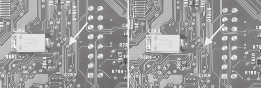
Figure E-1: Left, arrow points to the original pad that is being soldered. Right, pad has been torn off through excess heat and force.
The strategy for recovering from a broken trace is to remove the soldermask, fix the trace with a jumper wire, and find an alternate point for soldering by following the trace to a nearby component or via.
Removing the soldermask reveals the underlying copper traces. A short jumper wire can be soldered to these bared traces to fix the discontinuity caused by the torn trace. The bare region also serves as a convenient starting point for using a continuity meter to find an alternate point for affixing the jumper wire. Remove the soldermask using either a fine-grit (200 or finer) sandpaper, or by scraping the surface with a sharp hobbyists knife. When removing the soldermask, be careful not to catch pieces of the broken trace and further tear the trace of the board. Once the soldermask has been removed, clean the region with a gentle solvent, such as rubbing alcohol, using a cotton swab. Then, apply a very thin layer of soldering flux to the region and rub a clean soldering iron tip along the exposed traces. Small amounts of solder sticking to the iron’s tip will wick onto the circuitboard and coat the traces, preventing oxidation of the bare copper. If the iron’s tip is too clean, apply a drop of solder to it and lightly wipe the tip off on a wet sponge and try again. Do not attempt to tin the exposed traces with a ball of molten solder on the tip. Excess solder will be deposited that can lead to shorts. (Note that the soldering flux is essential for getting a uniform, thin coating of solder on the traces. Do not skip the application of the solder flux.) Figure E-2 illustrates what the traces will look like before and after the tinning process.
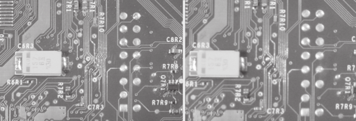
Figure E-2: Left, region after soldermask has been removed with fine-grit sandpaper. Right, region after it has been tinned (reconditioned for soldering).
At this point, you may want to use a continuity meter to determine an alternate point for attaching your modification wire. Most voltmeters come with an audible continuity meter function. When selected, a tone is emitted from the voltmeter whenever the resistance between the probes is very low.
Vias and component leads both make good alternate attachment points. If you decide to use a via, you must scrape the solder mask off and condition the via prior to attaching the modification wire. Figure E-3 illustrates using a continuity meter to find an alternate soldering point. Keep in mind that sometimes you will have to trace through several vias to find the best alternate attachment point.
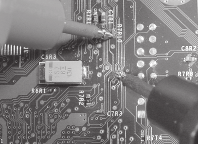
Figure E-3: Using a continuity meter to find an alternate attachment point. In this case, R7R10 turns out to be a good alternate.
The next step is to attach a short jumper wire across the broken trace. Apply a touch more soldering flux over the region of the broken trace. Cut a piece of fine wire (about 30-gauge) that is about the length of the gap in question. Place the wire over the gap, using the stickiness of the soldering flux to aid the placement process. Hold the wire in place with a pair of tweezers, and apply heat with the soldering iron until both sides have bonded to the edges of the broken trace. Verify that the wire is in place by gently pushing on it with the tweezers; the wire should not move. Also inspect for shorts to neighboring traces using your continuity meter. If a short is discovered, simply heat the jumper until it falls off the board and try again. Figure E-4 illustrates what the repaired trace looks like.
Finally, attach the modification wire to the alternate soldering point that was discovered previously using the continuity meter.
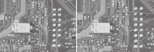
Figure E-4: Left, a jumper has been installed over the damaged trace. Right, the modification wire has been successfully attached to the alternate soldering point.