Appendix D -
Getting Started with FPGAs
Integration is the bane of hardware hackers. We like to take things apart, modify them, and improve them, but the trend has been to cram everything into one or two ASICs (Application Specific Integrated Circuit). This kind of integration is out of the reach of mere mortals, as the cost of a set of masks used for defining the features on chips is rapidly approaching one million dollars. That’s one million dollars per unique revision of the chip. If a mistake is made that requires a new mask set, you have to spend yet another million dollars to fix it.
Fortunately, a million dollars cash upfront for a chip is too much even for many corporations, and this has created a market for FPGAs — general-purpose, programmable (“reconfigurable”) hardware devices that can be used in place of an ASIC in many applications.
What Is an FPGA?
FPGA stands for field programmable gate array. In other words, it is an array of gates that can be programmed in the field by end users. You can think of FPGAs as custom silicon that you can build in the comfort of your own home, although the trend toward partial reconfigurability and context-sensitive reconfiguration adds a dimension to FPGAs that is not found in ASICs. While ASICs are cheaper per unit in volume, and they can have much higher clock speed performance, FPGAs have established themselves as the tool of choice for low to moderate volume applications and for prototyping.
The FPGA’s basic architecture is that of an array of hardware primitives embedded in a flexible routing network. The power of the FPGA comes from the fact that complex computations can be broken down into a sequence of simpler logic functions. These simpler functions can each be broken down in turn, until the entire computation is described by nothing more than a sequence of basic logic operations that can be mapped into the FPGA’s hardware primitives. Thus, the same FPGA can be used to implement a microprocessor, a video controller, or a tic-tac-toe game just by changing the configuration of the hardware primitives and the routing network.
The kinds of hardware primitives implemented by an FPGA architecture strongly influence the FPGA’s implementation efficiency for a given target application. Modern FPGAs provide designers with mostly one bit wide primitives: a 4 or 5 input to 1-bit output lookup table, and a single bit of time-synchronized storage known as a flip flop. Lookup tables are used as the logic primitive because they can be programmed to perform any logic operation with as many terms as there are inputs to the lookup table. These primitives are then wired into a vast programmable network of wires; a typical high-end FPGA might have many tens of thousands of these primitive elements.
It turns out that while single bit-wide structures are very general, they can be very resource-inefficient in applications where the natural data width is large. In particular, the area dedicated to the actual logic primitives is around 1 percent in many cases, with the remainder being configuration memory and interconnect. All of this wire is required to handle the many routing permutations that you might require for single-bit wide applications.
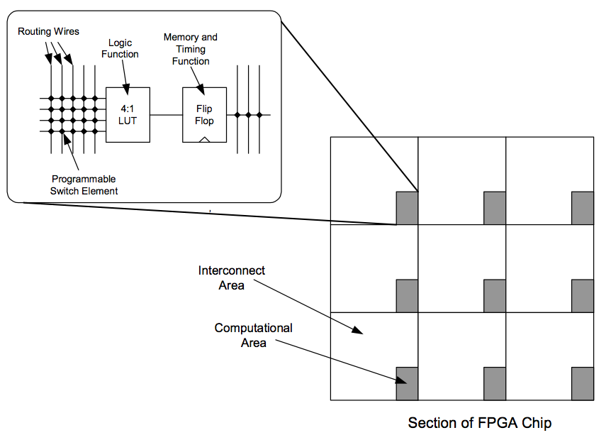
Figure D-1: Block diagram of a typical FPGA structure, illustrating the disparity between the amount of wire on an FPGA versus the amount of computational logic. A typical modern FPGA will contain several tens of thousands of these basic cells.
In order to boost area efficiency, many FPGAs also include a few coarse-grain primitives, such as chunks of RAM or a multiplier block. Xilinx’s Virtex II-Pro FPGAs even include several PowerPC cores on-chip. While this sounds impressive, the actual area consumed by such a core is surprisingly small: A PowerPC processor probably consumes a little more than 1mm2 of silicon area, whereas the area of the FPGA is hundreds of square millimeters.
The most recent FPGAs on the market have very flexible I/Os in addition to having very flexible computational hardware. A typical FPGA can interface to all of the most popular high-speed signaling standards, including PCI, AGP, LVDS, HSTL, SSTL, and GTL. In addition, most FPGAs can handle DDR clocked signals as well. In case those acronyms didn’t mean anything to you, the basic idea is that an FPGA can be used to talk to just about any piece of hardware you might find on a typical PC motherboard, such as the Xbox. This is extremely good news to hardware hackers, because it means that an FPGA can be used to emulate or monitor almost any chip found in a PC. (Of course, the PC may have to be down-clocked in cases where the FPGA cannot keep up with the speed of the PC.)
Designing for an FPGA
You have a number of design entry options to choose from for a typical FPGA design flow. If you prefer to think graphically, most design flows support a schematic-capture tool. While schematic capture is often more intuitive for hardware designs, they can be more difficult to maintain and modify. For example, changing al instances of a net name can be tedious if you have to click on every wire and type in the new name. Furthermore, the size of any single level of design hierarchy is limited to the size of a schematic sheet, so a complex design will require a good deal of planning and forethought for just the schematic capture.
As a result, hardware description languages (HDLs) are the tool of choice for implementing complex designs. HDLs look very similar at first glance to normal programming languages. For example, the syntax of Verilog looks very similar to that of C or Java. However, the semantics of the language can be a bit of a challenge to understand.
Hardware has an inherent parallelism that procedural languages such as C cannot express. If you think about it, every gate and every flip flop on an FPGA can compute in parallel, whereas in a C program, a single thread of execution is nominally assumed. As a result, HDLs represent hardware as a collection of processes that operate in parallel; it is up to the coder to group all of the functions into the correct processes so that the compiler can understand how to turn a process into gates.
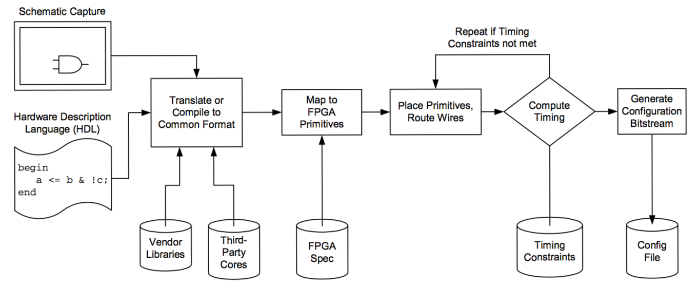
Figure D-2: Typical FPGA design flow.
For example, a single clocked storage element (a flip-flop) in Verilog is a “process” that typically has a structure similar to this:
input inData; // declare your inputs and outputs input clock; reg bitOfStorage; // declare the storage bit as a reg type always @(posedge clock) begin bitOfStorage <= inData; end
This code takes the value on input port inData, and on every rising clock edge, stores inData in a flip flop whose output is called bitOfStorage. Multiple processes delimited by always @( ... ) begin ... end syntax can exist in a single design, and all processes execute in parallel. Combinational logic can also be expressed as a process. For example, the following Verilog code implements a two-input multiplexer that has no clock:
input a; input b; input select; output out; reg c; always @(a or b or select) begin if( select == 1’b1 ) begin c <= a; end else begin c <= b; end end assign out = c; // assign statements can contain logic // functions as well
In this example, the contents of the parenthesized block following the always keyword contains a sensitivity list that includes all of the inputs that might affect the output. Leaving a parameter out of the sensitivity list means that the output will not change, even if that parameter changes. For example, if you omitted a and b from the sensitivity list, then the only time the output would change would be when select changed: you would have built a latch that stores either a or b depending upon the state of select. However, the desired operation of a multiplexer is to relay changes on either a or b to the output at al times, even when select does not transition, so a and b must both be part of the sensitivity list.
There are a number of subtleties when learning an HDL that are beyond the scope of this book, but the two code segments above should give you a flavor for what to expect. A skilled software programmer may have more trouble adjusting to an HDL than a novice, because many software tricks that are taken for granted translate very poorly to direct hardware implementation. Arrays, structures, multiplication, and division primitives are all taken for granted in the software world, but each of these constructs translate to potentially large and inefficient blocks of hardware. Furthermore, in a hardware implementation, all possible cases in a case statement exist whether or not you intend for it; neglecting to fully specify a case statement with a default case often means that extra hardware will be synthesized to handle the implicit cases. Numerous tutorials and syntax reference manuals for Verilog are indexed in Google; verilog syntax and verilog tutorial are both good sets of keywords to start out with when searching for syntax references or tutorials. Xilinx’s website also has a good Verilog reference for FPGA designers, and Sutherland HDL, Inc. has a free Verilog quick reference guide at http://www.sutherland-hdl.com/on-line_ref_guide/vlog_ref_body.html.
Overclocking FPGA Designs
It is worth noting that the timing models used for an FPGA are quite conservative. This means that it is quite likely that an FPGA will operate properly at frequencies much higher than the timing analyzer will admit. In fact, careful hand-layout of an FPGA’s logic can stretch the performance of the FPGA much further than its stated specifications.
For example, the FPGA (Xilinx Virtex-E) used to implement the Xbox Hypertransport bus tap is only specified to handle data rates of around 200 Mbits/s/pin, but the application demanded 400 Mbits/s/pin. The reason I could pull this off is that the actual logic and storage elements can run very fast, but most of the performance is burned off in the wires and repeaters that carry the signals between logic elements. Specifically, some wires will have so much delay at 400 Mbits/s that they effectively store data for a single clock cycle.
I determined which wires were slower than the rest by capturing a sequence of data and comparing it against a pattern that I had previously discovered using an oscilloscope. Once the slow paths were identified, I inverted the clock and/or inserted flip-flops on channels that had too little delay. The end result was a set of signals that were time-skew corrected. These signals could then be trivially demultiplexed to a lower clock rate where conventionally compiled HDL design techniques could be used.
While this technique is very powerful, it is not generally applicable because the amount of delay caused by a wire varies from chip to chip and can depend on parameters such as the ambient temperature and the quality of the power supply voltage. However, for one specific chip under controlled circumstances, I was able to get 2x the rated performance. Another important difference between this application and a more general application is that bit error rates on the order of 1 error in a few thousand was tolerable, since I could just take three traces and XOR them to recover any information lost to random noise sources. However, 1 in 10,000 bit error rates are not acceptable for normal applications; unrecoverable error rates better than 1 in 10,000,000,000,000 are more typical. This all goes back to a saying that I have: “It is easy to do something once, but doing something a million times perfectly is hard.”
Another advantage of the HDL design entry approach is the availability of free and paid “softcores.” Websites such as www.opencores.org offer general-public licensed HDL cores for functions such as USB interfaces, DES and AES crypto-engines, and various microprocessors. In addition, almost every standard function is offered by third-party vendors who will sell you cores for a fee.
After design entry, I highly recommended that you simulate your design before compiling it into hardware. Trying to track down bugs by twiddling code, pushing it to hardware and probing for changes is very inefficient. Simulation allows you to probe any node of the circuit with the push of a button. In addition, the effort required to simulate a code change is very small, especially when compared to the effort of pushing a change all the way through to hardware.
Once the design has been entered and simulated, it needs to be compiled or translated into a common netlist format. This netlist format is fed into a program that maps the netlist primitives into the target FPGA hardware primitives, after which the mapped primitives are placed and routed. The resulting design is analyzed for compliance with a set of constraints specified by the designer. If the design does not meet the designer’s specifications, it is iteratively refined through successive place and route passes. Once the design passes its design constraints, it goes to a configuration bitstream generator where the internal representation of the FPGA is translated into a binary file that the FPGA can use to configure itself. (All of these steps happen fairly seamlessly at the touch of a button in the later versions of the FPGA design tools.)
Project Ideas
Now that you know a little bit about what an FPGA is and how you can program them, what sorts of things can you do with them?
As it turns out, FPGAs have enough logic capacity and performance these days to accomplish a very impressive range of tasks. The obvious industrial application of FPGAs is in the emulation of designs intended for hard-wired silicon. The cost of building a custom chip has been skyrocketing, and it will soon be the case where a single critical mistake can cost hundreds of thousands of dollars, if not millions, to fix.
On the other hand, fixing a mistake made in an FPGA HDL description pretty much only costs time and design effort; you don’t throw away any parts, and you don’t have to buy any new parts. Thus, many companies have adopted the strategy of fully simulating a mock-up of the design in FPGAs before taping out the final silicon. A side benefit from this approach is that the software and hardware teams that are users of the custom silicon can begin validating their designs using the FPGA mock-up while the custom silicon is being fabricated; a process that can sometimes take a couple of months.
For hackers, FPGAs are sort of a panacea for all kinds of complex projects. They are excellent choices for implementing cryptographic functions if you are interested in doing brute-force keysearches or encrypting large amounts of data quickly. They are also very useful for implementing signal processing functions, especially given the existence of free multiplier and digital filter cores. FPGAs can achieve higher performance for less power than a DSP, and thus they have a unique niche in applications such as battery-powered robotics. FPGAs are also useful for embedded controller applications: A small microprocessor core, equivalent to or better than a PIC, can easily fit in an FPGA today. Add all your custom hardware peripherals, such as a serial port and PWM timing generators, and you’re in business.
FPGAs are also useful in situations where the focus is not on big number crunching. An FPGA makes a great piece of glue logic in a tight spot, and well-placed FPGA can save you from having to ever add a wire jumper to patch a board due to a logic design error. FPGAs also make a cheap logic analyzer alternative for those of us who cannot afford a $10,000 Tek TLA mainframe. The high-speed I/O capabilities of the latest FPGAs combined with large autogenerated FIFO-configured embedded memories make short work of designing a signal capture and analysis system.
Finally, FPGAs have applications in mixed-signal situations that are not immediately obvious. The most common mixed-signal application is probably using an FPGA to drive the analog signals of a VGA monitor. A couple of resistive dividers or a well-chosen output driver type is all you need, and al the timing and logic necessary to generate color images can be handled with logic inside the FPGA. FPGAs can also be trivially used as PWM D/A converters, or even as part of a sigma-delta D/A or A/D converters.
Where to Buy
You’re probably thinking that any tool this versatile and powerful has to cost a fortune. While that was true about a decade ago, today you can buy 100,000 gate FPGAs for well under $50, and the design tools are often free for educational users and/or hobbyists.
Of course, an FPGA on its own is not so useful; it needs to be mounted to a board with the proper connections in order to be used. To this end, a company cal ed XESS (www.xess.com) makes a line of fairly affordable FPGA starter kits. Their product line shifts as new FPGAs are introduced, but the current entry-level FPGA board is the XSA-50 board that comes with a 50,000 gate FPGA for about $150. The board also includes a few megabytes of RAM, a parallel port, a VGA port, a PS/2 keyboard port, and a few other essential items.
The other option is to build your own board from scratch, if you’re feeling bold. Other appendices in this book describe how to get into board layout and fabrication and how to attach fine-pitched FPGA devices to your boards. It is actually quite rewarding to try to build your own boards, and I recommend giving it a try; the cost of fabricating a board is well below $100 these days, so you don’t lose too much even if your board doesn’t work in the end.
If you are making your own board, you will need to buy your FPGA from a Xilinx distributor. The Xilinx webpage (www.xilinx.com) has the most up-to-date links to distributors. As of this writing, one of the more convenient distributors is NuHorizons (www.nuhorizons.com), as they offer product availability and pricing information on their webpage without requiring registration or a special customer account.
FPGA development software can usually be acquired at a low price or for free. For example, Xilinx offers a free development environment for its Virtex-II (up to 300K gates), Spartan II-E and CoolRunner lines of parts. The development environment is called the Xilinx ISE WebPACK, and it is available for download after registration at www.xilinx.com. This free environment sports an impressive list of features, including schematic and HDL input, HDL synthesis, a flooplanner, timing driven place and route, timing analysis, and power analysis tools.
Xilinx also offers a version of its software called “Xilinx Student Edition” through Prentice-Hall. This software comes bundled with a number of tutorials and documentation that can help you get into FPGA design. You’ll find a wide variety of helpful tutorials and lectures on the Xilinx website under the “Education” tab.