Appendix C -
Getting into PCB Layout
This appendix will introduce you to the PCB design and layout process, and will survey available tools that you may need to achieve your design goals, featuring products and techniques for those on a shoestring budget. I conclude by presenting some simple designs to get you started in your hardware adventures.
Philosophy and Design Flow
Printed circuit boards are the canvas of the hardware hacker, and CAD tools are the brushes. Like any engineering or artistic discipline, building profi-ciency in printed circuit board design and layout takes practice. Fortunately, the advent of inexpensive PCB prototyping services and free (or nearly free) CAD tools have made PCB design and layout an inexpensive and accessible hobby.
The design and layout of PCBs are two intimately coupled tasks. Trade-offs give and take throughout the design and layout phases. Sometimes a component may not fit, or a part may not be available, and you’ll have to change the schematic design to allow for this shortfall. Other times, you may make a high-level design change or you may catch a bug, and the PCB will have to be updated to reflect these changes. In my experience, the key to rapidly cranking out a successful PCB design is to be flexible on all design fronts.
Refining Your Idea
The PCB design process always starts with your idea. The first thing you need to do is to get a very clear vision of what you are trying to build. The more specifics you have up front, the easier you will find the design process. You should have an idea of how big you want the final board to be, how much it should cost, and of course what it should do. I always find it helpful to draw sketches and, in the case of large projects, to write design documents that help me organize and record my thoughts.
For the first few designs, one of the most difficult steps will be nailing down an idea, because you won’t know what kinds of components are available to implement your idea, and what sorts of real-world constraints you will have to design around. The best way to get started is to find an existing idea that is very similar to yours and to model your idea after it. (Many chip manufacturers offer free application notes and design samples that form a great starting point.) Another way to define your ideas is to learn from existing products: If you want to build an alarm clock, take an existing clock apart to see how it was built.
Schematic Capture
Once you have your idea, you need to create a schematic diagram. A schematic is a symbolic representation of your idea, expressed as a collection of part symbols and virtual wires.
Most schematic capture software comes with a library of parts to help accelerate the schematic capture process. However, if you do not find the part you need in the library, you will have to build your own schematic symbol. All schematic symbols are linked to a PCB component footprint, which is a pattern of copper on a PC board that mates to a component.
One common source of errors stems from not checking the link between the symbol and the footprint: A 16-pin DIP footprint does not fit a 16-pin in-line surface mount connector, and most design tools cannot tell the difference between the two. Therefore, check to make sure that your footprint assignments are all correct, and double and triple check the schematic symbol. In particular, always check and recheck power pins, since they can cause the most difficult and destructive kinds of errors. Consider having a friend double check the symbols as well, to avoid repeating errors or allowing errors to pass unknowingly. (This amount of redundancy may sound silly for simple parts, but it becomes absolutely essential for hundred and thousand-pin parts where your brain becomes mush halfway through the checking process.)
Attention to detail from the very beginning is the most important skill for capturing a schematic, and can save you from the headache of frustrating bugs later on. Every pin on every component is there for a reason, and if any pin is left unconnected you should understand why that is or is not okay. To this end, read the product data sheets, including every single page and footnote. Don’t ignore the fine print that requires a pull-up resistor to set startup conditions, or a capacitor to filter noise or stabilize the system or you’re likely to end up with more frustrating bugs.
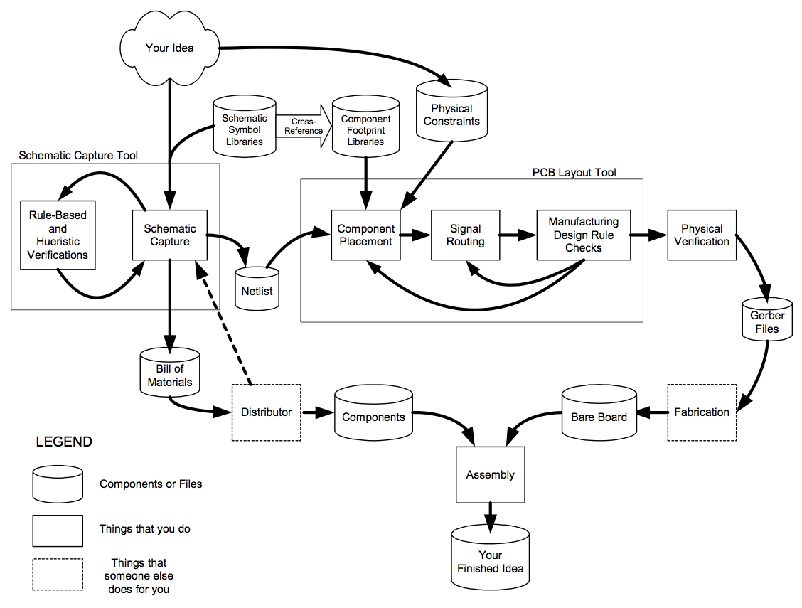
Figure C-1: The board design process, from idea to finished product.
Design rule checkers are helpful in finding some errors in schematics, but the checks they perform are usually quite elementary, and thus catch only the grossest of errors. A typical set of checks might include catching duplicate part designators, dangling nets, and floating inputs.
In addition to conventional design rule checkers, you can also devise your own simple checks. For example, many design tools do not perform “netlist parity checks,” which can be generated fairly easily using a perl script or a spreadsheet program. Netlist parity checks are heuristic checks that tally the number of components connected to each netlist, then sort the tal y by the number of connections. The “single-pin nets” will be at the top of the sorted list. A single-pin net is almost always an indication of a typographical error (misspelled netlist name) during schematic capture. It can be useful to browse through the whole sorted list briefly, to see that all groups of signals have the same number of connections. Most signal busses have the same number of connections to every signal in the bus. You can create a tool that enables netlist connection tally checks for your schematic capture program in an afternoon, and you will undoubtedly save yourself countless hours of effort and money by finding the bugs it will catch.
Before exporting the schematic to the board layout tool, you should order all of the parts in the schematic’s bill of materials. Often, critical parts will be in short supply and the schematic capture wil have to be redesigned to account for the shortage. Frequently, a change in a component footprint assignment is the only redesign necessary. Modifying the schematic design to account for manufacturer’s shortages avoids the difficult task of making the change on a finished board layout.
Board Layout
The input to a board layout program is a netlist that is annotated with component footprint information. A netlist is an intermediate representation of every component and pin, and their connectivity. Netlist extraction is a well-automated process, but the correlation of schematic symbols to PC board footprints is not always well-managed.
The difficulty of symbol-to-footprint correlation stems from the availability of multiple packaging options for a single part. For example, the symbol for a transistor could equally imply a tiny SOT-23 packaged device or an enormous TO-3 packaged device, and it is up to you to ensure that the proper package is chosen during netlist extraction. It’s always good to check the implied footprint when the component is placed in a schematic, rather than checking all at once during the netlist translation, or, worse yet, during placement or final design review.
Once you have a finished netlist, you are ready to do the board layout.
The other external input to a board layout program are the design rules. Design rules are set by the board fabrication company and include specifications for the minimum trace width and minimum trace to trace spacing, minimum hole size, minimum through-hole annulus, and the number of power and routing layers. The exact design rules depend on the process you choose, which in turn is driven by what you can afford. The best processes offer traces as fine as 2 mils (a mil is 1/1000th of an inch or 25.4 microns) and laser-drilled blind/buried vias with a diameter of about the same, but the price for fabrication is well outside the typical hobbyist’s budget of less than one hundred dollars. A more typical hobbyist’s process features 6 mil trace/space design rules with 15 mil minimum finished hole sizes, with either two or four layers of copper. (You’ll find a list of board fabrication companies toward the end of this appendix.)
Board layout consists of two phases: placement and routing. Intelligent parts placement will greatly simplify the routing task. In general, the goal is to place all parts so as to keep connections as short as possible, with as few vias as possible, in order to minimize noise, delay, and signal losses. The placement of some parts, such as connectors, switches, and power components, are well-constrained, leaving you little choice. For the remainder of the parts, an understanding of the design will help you to determine which parts should get the best placement.
Once your placement is finished, print the design at a scale of 1:1 and verify that the components fit in their respective footprints by populating the printed layout with the actual components. If you intend to use a socket with a component, be sure to use the socket for verifying the 1:1 plot, as sockets require more space than the component itself. This check guarantees that you have all the components in the correct package type, that all your component outlines are correct, and that there is sufficient clearance between each component to facilitate easy assembly. Another important thing to check on the 1:1 plot is the orientation and pinout of all the connectors because it is very easy to invert a connector or to have used the wrong gender’s footprint on the circuit board. Be careful when handling chips too, especially those with fine-pitch surface mount leads. Be sure not to bend the leads, and observe proper static electricity control protocol.
General Placement and Routing Guidelines
Here is a short list of some placement and routing guidelines. Remember, these are just general suggestions, and there will undoubtedly be situations where they do not apply.
Leave Space for Via Fanouts on Surface Mount Devices
Surface mount devices offer a great density advantage when compared with the older through-hole componentry that used to be the de facto standard. However, surface mount components still require through-hole vias for routability, especially in complex and/or auto-routed designs. These routing vias are referred to as “fan-out” vias for SMD pads. Figures C-2 and C-3 demonstrate the use of fan-out vias on a surface mount part.
Decoupling Capacitors Fit Nicely Under SMD Pads
The most common passive component in a typical digital design is the decoupling capacitor. These tiny capacitors are everywhere, and they can consume valuable routing and via fan-out space if they are not properly placed. If you are willing to create a double-sided surface-mount board, decoupling capacitors can be placed on the board side opposite the target component’s pads. By placing these components under the component’s pad space, you are not consuming any via fan-out area. In fact, a well-placed decoupling capacitor can share the power via used by the component’s power pins. The view in the lower left hand corner of Figure C-2 provides a clear illustration of this technique. (There are some special cases where you may not want to do this, as noted in the next section.)
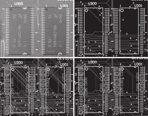
Figure C-2: Four views of a circuit board layout. From the top left, clockwise: fabricated circuit board with components; top-layer circuit board view in PCB layout program; all-layers circuit board view in PCB layout program; top and bottom only layers view demonstrating two-sided SMT layout.
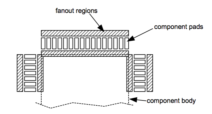 Figure C-3: Fan-out regions around an SMD component’s footprint.
Know Your Special Traces
The good news about laying out digital circuit boards is that most traces require little thought, unlike a typical analog board. The bad news is that if you don’t do the rest of the traces correctly, your board will exhibit strange and frustrating behavior that will be hard to debug. As a result, routing these special traces is a little bit of a black art. This section gives just a few guidelines for coping with these special traces, but I encourage interested readers to find a text dedicated to board layout to really learn and appreciate these techniques. Two texts that I recommend are Digital Systems Engineering by William J. Dally and John W. Poulton (Cambridge University Press), and High Speed Digital Design: A Handbook of Black Magic by Howard W. Johnson and Martin Graham (Prentice-Hal PTR).
Typically, the kinds of traces that require special attention when routing a circuit board are:
- Power traces
- Timing reference (clock) traces
- High speed traces
- Analog/mixed signal traces
As a general rule, power traces should be thicker than your average signal trace, especially if you are using one of the higher-end fabrication processes that offer narrow (~ 5 mil) trace widths. Power traces need to be thickened to counter both resistive heating and parasitic inductance. Narrow power traces, especially near the key power distribution points, will act like resistors and heat up, dropping the supply voltage to a level that causes indeterminate malfunctions in your circuits.
The proper sizing of a power trace depends upon the thickness of the copper. Typical boards use “1-oz copper” that is 1.35 mils thick (one square foot of 1.35 mil thick copper foil weights one ounce). An exterior 12 mil wide trace in 1 oz copper is required to pass 1 ampere of current with a 10 degree Celsius temperature rise. Thicker traces are required for buried layers for a similar current handling capacity.
When routing power traces between layers, remember that vias have resistance as well. A single via is insufficient to connect critical power traces between layers. Critical power traces should have multiple vias connecting them between layers to keep parasitic resistances and inductances down. Distributed power planes on multiple layers should also have vias generously distributed throughout to ensure that a common potential is preserved.
Note

In high performance or low noise applications, placing a via between a decoupling capacitor and the power pin may carry too high an electrical integrity price for the routing convenience. Vias disrupt the propagation of high-speed (hundreds of megahertz) electrical waves. Thus, the optimal location of a decoupling capacitor in these applications is between the component pin and the power via.
Timing reference signals include clocks and strobes. Many memory devices require asynchronous control strobes that have sensitive timing requirements. These signals should be properly terminated and routed in a manner consistent with the termination strategy, typically a “daisy chain” route. Daisy chain routes have no branches, so there is only one path for the wavefront of the signal to travel.
Electric signals travel at about 1/4 the speed of light on a circuit board, or about three inches in a nanosecond. Thus, high speed traces must have matched lengths, or signals can arrive significantly out of phase with respect to the timing reference. Trace lengths are matched by extending shorter traces to the length of the longest trace. Trace length extension is accomplished using serpentine traces that meander and increase the effective length of a trace without changing the placement of the trace’s endpoints.
Analog and mixed-signal routing is well beyond the scope of this appendix. In an average hobbyist’s digital design, most of the analog circuitry will be isolated to the power supplies. Any special layout requirements for a particular power supply component is typically well-documented in the component’s datasheet.
Keep in mind that electrical signals are lazy and promiscuous: signal current will always follow the path of least resistance, and signals will couple into adjacent traces. Furthermore, current must be conserved, so every signal current path must have a return current path, whether it is explicit or not. Keep these simple rules in mind as you layout any analog sections on your circuit board.
Circuit Boards Make Fine Heatsinks
When routing high-power components, such as power regulators and high-performance microprocessors, remember that the copper in a circuitboard is an excellent conductor of heat. You can save yourself a heat sink under certain conditions by simply laying out a large region of copper connected to the heat slug or ground pins of the target part. If you are using a multilayer board design with power planes, use multiple vias to help conduct heat into the internal layers.
The heatsinking capabilities of a circuitboard can also be a nuisance during hand assembly. The good thermal conductivity of copper makes it difficult to heat up a component pin that is also connected to a large region of copper. When connecting low-power components to the power planes, consider using vias with thermal reliefs. A thermal relief is a set of small gaps in a via connection to a power plane that reduces thermal conductivity without significantly impacting the connection’s electrical performance. (Note that a large group of densely packed thermally relieved power vias around a region of copper can result in unconnected or poorly connected islands of copper.)
Establish Preferred Routing Directions for Each Layer
Establishing a dominant routing direction for each layer can simplify the routing of dense boards. For example, make the top layer the horizontal routing layer, and the bottom one the vertical routing layer. If you need to route a signal between two components located diagonally across the board, first run a horizontal trace on the top and then a vertical trace on the bottom to connect the two components. The alternative strategy of just running a trace diagonal y across the top layer of the board, for example, reduces the overall routability between the two halves of the board by one-half: The only way to get from one half to the other is now to go on the bottom.
Exceptions to this rule are acceptable, especially if you have to make a signal integrity versus routability trade-off.
Stack a Board with Orthogonal Layers
After establishing the preferred routing directions for each layer, stack the layers such that no two layers have parallel preferred routing directions. This orthogonality helps keep the interference of signals between layers to a minimum. If you have power layers, try to stack them between layers to help shield interference between signal layers.
On Two-Layer Boards, Use Fingers to Bus Power
On a two-layer board, it is often tempting to just run power and ground as a ring around the outside of the board. This is not an ideal situation, because the ring starves the heart of the board and also increases the potential for large parasitic current loops that will degrade circuit performance. Instead, use interdigitated and/or stacked power fingers.These fingers will establish the dominant routing direction of each layer, and should be laid out before routing any signals.
Hints on Using an Auto-Router
Auto-routers are a mixed blessing: they can save hours of routing time, but they can also cause hours of frustrating problems. The first rule of using an auto-router is to never allow it to work on your only copy of a circuit board design file. Instead, create a copy of your design and let the auto-router perform its magic on the copy.
The second rule is to learn the auto-router’s bugs using simple test designs before applying it to your final design. Auto-routers frequently have critical bugs or limitations that must be understood before using the tool. When learning an auto-router’s bugs, pay particular attention to how it handles locked traces, poured polygons, and awkward trace sizes. Some auto-routers will actually remove locked traces (traces laid down by hand and marked as unmovable), while others ignore them or do not function in their presence. This can be particularly frustrating if you have spent hours laying out the critical power and timing nets before turning on the auto-router.
Finally, don’t count on an auto-router to fully route a complex board. Auto-routers are great for quickly routing the first 90 percent of a board, but they really slow down as the board gets more congested. Note that subtle changes in component placement can make or break an auto-router. Many auto-routers will not recognize busses or straight-through connections without special annotation or ideal component placement.
CAD Tools
Board design tools have dropped in price significantly over the past few years. The tool I use most frequently for board design is Protel 99SE. (I have yet to purchase the newer version, Protel DXP.) Protel is a highly integrated tool, featuring schematic capture, simulation, library management, and board layout with design rule checking and auto-routing, all integrated in one tool. (It seems like every software release some new feature is integrated into the design environment, for better or for worse.)
You can download a 30-day fully functional demo of the Protel software from their website at www.protel.com. While a full-fledged license for the product is in the thousands of dollars, this still compares favorably with many other software packages that offer the same depth of functionality and number of features. Other high-end PCB CAD vendors include
Mentor (PADS), Cadence (OrCAD), and Altium (P-CAD). Interestingly, Altium also owns the Protel software suite.
If you are are just starting out and want to do some casual board layout, some board fabrication companies offer full-function captive design tools for free. ExpressPCB (www.expresspcb.com) offers a free schematic capture and PCB layout tool for clients who use their fabrication service. Their tool is functional, but a little limited in terms of the design rule checks and the practical complexity for which you can realistically use it. ExpressPCB is a great starter tool for beginners, however, and is capable of implementing almost any weekend hardware project.
Before submitting any finished design for production, preview your exported files with a third-party file viewer to help protect your fabrication investment against bugs in your design tools. The most common file format used for board fabrication is the “Gerber” file format. A good, free Gerber previewer that I trust is made by Graphicode (http://www.graphicode.com/).
Board Fabrication Companies
Board fabrication companies come in as wide a range of capabilities as the CAD tools. Some companies only do large production orders, while others earn their bread and butter servicing the quick-turn prototype and hobbyist market. Here are a few of my favorite board fabrication companies, along with a brief description of their basic offerings.
Sierra Proto Express
Located in San Jose, California, Sierra Proto Express offers some of the most competitive quick-turn prototype rates. As of this writing, Sierra Proto Express offers a line of “No Touch Product” processes. These fabrication processes have strict design rule requirements, but they are very affordable. For example, you can have a two-layer circuit board fabricated in four days for $34 per board (minimun order of two boards), or you can have a four-layer circuit board fabricated in four days for $51 per board (minimum order of two boards). The technology offered at these prices is a 6 mil trace/space design rule with 15 mil finished hole sizes. Sierra Proto Express also offers faster turn-time processes with trace widths down to 5 mils and 10 mil finished hole sizes. For more information, visit www.sierraprotoexpress.com.
Data Circuit Systems
Data Circuit Systems, also located in San Jose, California, is my vendor of choice for designs that require aggressive design rules or special processing options that don’t fit well with the cheaper quick-turn companies’ offerings. Their comprehensive “Process Capabilities Survey” (available for download at their website) is comprehensive and clearly written, so it takes a lot of guesswork out of interpreting the design rules. They also do a fairly rigorous set of factory checks on your submitted design, which often catch subtle layout errors that can cause problems later. I have found their staff to be competent and friendly and, though their prices are slightly higher than most engineering prototype manufacturers, their well-documented process and design rule checks help reduce the risk of aggressive designs, and in the end the extra cost is probably worth it. Visit www.datacircuits.com.
Advanced Circuits
Advanced Circuits of Aurora, Colorado (www.4pcb.com) features an instant quotation feature at their website. This feature alone makes them a good choice for boards of intermediate-complexity that do not fit any of the discount, quick-turn process guidelines. You can use the instant quote feature to optimize your choice of implementation technology for price. In addition, they frequently offer discount, quick-turn specials.
Alberta Printed Circuits
Alberta Printed Circuits (AP Circuits), located in Alberta, Canada, is one of the original quick-turn prototype PCB houses, with prompt service. The P1 process they offer is a basic one, with no soldermask or silkscreen. As a result, it is difficult to execute fine-pitch surface mount designs because solder tends to get everywhere during the assembly phase. However, they will fabricate and ship your board in the P1 process in just one day for an unheard of price, with no minimum order requirements. The base fee for a production run is about $45 at the time of writing, with approximately a $0.65 per square inch charge on top of the base fee. The technology is an 8 mil trace/space with a minimum drill size of 20 mil (28 mil if you want to stick with the cheapest process option). AP Circuits is great for boards that have to get done in a pinch and on a strict budget, especially if you are using through-hole or coarse SMT components that are easy to assemble without a soldermask. Visit www.apcircuits.com.
Starter Projects
In Chapter 5, “Replacing a Broken Power Supply,” you are instructed on how to replace an Xbox power supply with a standard ATX power supply. The one problem is that the polarity of the power on signal is inverted between the Xbox and the standard ATX supply. The hack solution proposed in the chapter is to always leave the supply on, and to instead switch the Xbox on and off by first turning on the power supply and then pressing the Xbox’s power button.
It is fairly easy to design and layout a board that enables you to invert the polarity of the power signal so that you can control the power state of the Xbox from just the front panel of the Xbox. You can also properly regulate the standby power supply, instead of using two diodes. Such a board would consist of an inverter chip, such as the 74HCT04, and a regulator, such as the LM317K. The LM317K is an adjustable regulator that can be set to reduce the +5V standby voltage provided by the ATX supply down to the +3.3V standby voltage demanded by the Xbox. An example schematic diagram of this board is shown in Figure C-4.
The choice of connectors to this board is up to you. The simplest solution would be to just use holes and solder the wires through the holes. There are only five connections on this board. Three go to the power supply: the +5VSB (violet) wire, a ground (black) wire, and the power on output (green) wire. The remaining two, +3.3VSB (pin 6 on the power connector) and power on input (pin 11 on the power connector), go to the Xbox.
Be sure to test the voltage output of the regulator before installing your finished board. It is fairly easy to get a resistor value wrong or a pin swapped, and both of these conditions could lead to dangerously high voltages going into the Xbox. Also, when installing the board permanently, be sure to insulate the bottom and top of the board from accidental contact with the Xbox case or other Xbox components.
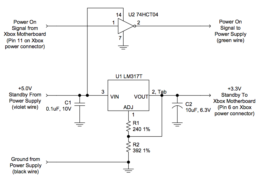
Figure C-4: Example schematic diagram of the ATX power supply replacement adapter board. Resistors R1 and R2 program the output voltage of the voltage regulator, U1, to be +3.3V.