Appendix B -
Soldering Techniques
This appendix will explain the basics of soldering as well as some more advanced surface-mount soldering techniques. You will get the most out of this appendix if you experiment with the soldering techniques as you read along. Jameco Electronics (www.jameco.com) sel s a wide variety of project kits requiring through-hole assembling that you can use for basic soldering practice. Companies such as TopLine (www.topline.tv) offer economy practice kits using component blanks if you want to practice your SMT assembly techniques, and MCM Electronics (www.mcmelectronics.com) offers a practical Surface Mount Solder Practice Kit. (I highly recommend that you practice your SMT soldering skills before trying to attach an SMT component that you care about.)
Introduction to Soldering
The basic technique for soldering is fairly easy: wedge the tip of your soldering iron into the space between the component lead and the circuit board pad to heat both pieces up. Once they are sufficiently hot, gradually feed some solder wire into the joint until a nice, smooth solder fillet is created. In reality, soldering requires a bit of practice and experience before one is able to solder a typical board with over a thousand joints without any bad solder joints. In order for a good solder joint to be created, the hot liquid solder must “wet” the subject pieces in order for a connection to be made. Thus, the real art of hand-soldering is understanding how to guarantee solder wetting.
You can tell when liquid solder is wetting a piece of metal by looking at it. A wetted joint looks like the molten solder has lost all surface tension; the liquid solder is shiny and it flows smoothly over the work area. In the opposite situation, the solder has a dull sheen to it, and it tends to ball up around the soldering iron tip instead of flowing outward.
Use Flux
Solder fails to wet the subject metal because oxygen in the air or dirt and grease have reacted with the metals. In this case, you can apply a flux to your workpiece to break down these foreign compounds. The word flux comes from the Latin fluxus, which means flowing. Most solder comes with a core of flux built in to enhance solderability. If you look at a cut piece of solder carefully, you can see the flux core surrounded by the solder alloy. Always use solder with a flux core, or you will be in a world of pain trying to get the solder to wet. Almost all solders made specifically for electronics have a flux core, but there are solders that you can accidental y purchase in a hardware store that have no flux, and that are made for purposes such as joining pipes. When you heat a flux-core solder, a small puff of vaporized flux smoke will rise up. A small fan placed near the work area will blow the fumes away and prevent inhalation.
A common novice mistake is to have too much faith in flux-core solder. Frequently, the flux contained in a flux core solder is not enough to get the solder to wet. In this case, you will need to apply extra flux. Raw flux comes usually as a liquid or a paste, so application is easy. In liquid form, a single drop of flux can be applied with half of a toothpick. Break the toothpick in half, leaving the break slightly jagged. Dip the broken end of the toothpick into the flux, and a small drop will cling to the end. Applying liquid flux to a large area can be done with a fine-tipped artist’s brush, but be sure to clean the brush when you are done or it will end up gummy and unusable in a couple of days. A flux dropper is also handy, but expensive. A flux dropper is a bottle with a thin capillary needle on top; when you invert the bottle, flux slowly drips out of the capillary. In paste form, flux can be applied by dipping any piece of scrap, such as a toothpick or a piece of solid wire, in the flux paste. Finally, flux pens are handy for beginners because they combine flux storage and dispensing in a convenient and inexpensive package. Flux pens don’t have the accuracy or quality of other flux application techniques, but they are convenient and good for occasional use.
Many fluxes require clean-up after use. Fluxes can harden with time, making repairs difficult in the future, they can slowly attack the board, and they can absorb water and become conductive. The traditional soldering flux is a resin flux. Resin fluxes require the use of strong solvents that are flammable and toxic. As a result, I tend to recommend water soluble fluxes or no-clean fluxes. Water soluble fluxes can be removed by just washing down the board with water. It is better to use distilled deionized water, but I have found that most warm tap water is pretty effective as well. When I have to clean a large batch of boards, I throw them into a dishwasher (with the food trap cleaned and no detergent!). After the boards are washed, set them on a conductive, clean cookie sheet or aluminum foil, and put them into an oven on low heat (around 200°F) to bake for about an hour or two, or until all the water is driven away. Be sure not to turn the oven up too high, or water trapped inside the pores of components will turn into steam and cause them to crack or explode. Most parts are designed to be “process sealed” so washing them with water is fine. Be careful with connectors and switches, however; you may need to tape over them with a piece of Kapton tape to prevent contamination with water.
Warning

Do not use acid-type fluxes on circuit boards. They will attack the board and components and cause failures with time. Acid fluxes frequently plague novices who use solders and fluxes that are intended for pipe soldering.
Starter Tips
Components with many leads need to be aligned and tacked in place before soldering. If the component is of a surface-mount type, it can be held in place by soldering down two pins on opposite corners of the device. After tacking the component in place, re-inspect the alignment in case the component drifted during the tacking process. If the component is of a through-hole type, you will need masking tape to hold it in place while you turn the board over. Tack the corner leads of the component in place, and check that it is level to the board before soldering all of the leads. (Masking tape has a bit of play in it and frequently you will have to heat one of the tacked corners while pressing down on the component to level the component with the board.)
Kapton tape is a fairly handy thing to keep around the workbench. Made by DuPont, Kapton can withstand temperatures up to 500oF, well above the melting point of solder. It is handy for masking off nearby regions where you do not want solder. However, Kapton tape is expensive so use it only in situations where it will come in contact with hot solder.
Solder fails to wet metal that is too cold. This is a common problem when soldering large joints, or when soldering joints attached to large sheets of copper. In these cases, the connected metal conducts enough heat away so that the junction never reaches the melting point of solder. The solution to this is either to use a more powerful soldering iron (but be careful—the heat of very large soldering irons can also cause the board traces to fal off), or to leave your soldering iron in contact with the junction for a longer period of time before applying the solder. One trick to heating up the work area faster is to feed just a touch of solder into the tip of the iron where it is heating things up. Even though the solder will not wet on the board, the liquid solder on the iron’s tip increases the effective contact area between the iron and the board, and heat will be transferred more rapidly into the board.
After applying solder to the iron’s tip, you will sometimes have to rotate the iron, maintaining contact at the joint, in order to get the molten solder in contact with the board. You can tell when a component lead or a board pad is sufficiently hot by carefully observing the way light reflects off of it. Component leads and pads on a circuit board typically have some kind of plating on them, usually made out of solder. This solder plating has a slightly dull sheen under normal conditions. When made sufficiently hot, however, the sheen goes from dull to almost perfectly reflective. To get a feel for what this looks like, try heating up a large square pad with your soldering iron, using the technique described above. You can usually watch the melting front propagate across the pad as the soldering iron heats the board.
Warning

If you are using a non-temperature controlled soldering iron, use the lowest wattage soldering iron you can to get the job done. This will help prevent board damage, as excess heat can cause the copper traces to delaminate from the board.
Surface Mount Soldering
Mastering the skill of surface mount soldering requires a bit of patience, practice, and good tools. The basic tools that are required beyond the basic soldering kit are tweezers and a magnifying lens.
A good pair of fine-tipped tweezers is an essential soldering accessory for surface mount components. Tweezers are required for the safe handling of surface mount components during soldering, as small components will rapidly heat up and become hot enough to burn your finger. Tweezers are also necessary to hold small components in place, preventing them from being pulled around by the surface tension of the liquid solder as it melts and cools. The point on the tweezers should be small enough to fit in between the pins of the finest surface-mount part that you intend to work on. This way, you can use the tweezers to manipulate individual pins during soldering and inspection.
There are many grades of tweezers. The grading is based on the sharpness, quality and durability of the tips, the alignment of the tips, and the spring action of the tweezers. High-grade tweezers are a little bit pricey, but well worth the investment if you intend to do a lot of surface mount soldering. Distributors that focus on production supplies, such as Future-Active Electronics (www.future-active.com), sell a reasonable selection of good tweezers.
The biggest challenge in surface mount soldering is being able to see what you are working on. Your hands have the ability to easily and repeatedly manipulate objects smaller than the naked eye can see. The ideal magnifying solution for soldering is an optical stereoscope, like the kinds used for the inspection of biological specimen. Unfortunately, these microscopes are very expensive, with the better models selling for around the priceof a used car.
A more economical solution is to use a tabletop magnifying lens. Many drafting/art supply stores sel these kinds of lenses, and most office supply stores sell at least one model of lamp with an integrated magnifying lens. These magnifying lenses will help assembly, but they lack the power to do a thorough inspection of your soldering job. A relatively inexpensive high-power portable magnifier, such as a jeweler’s loupe or a proofing magnifier, should be used to inspect finished solder joints.
Technique for Simple Components
Simple surface mount components, such as resistors, capacitors, inductors, and small semiconductor devices such as transistors and diodes, are easy to mount on a circuit board. Let’s look at the technique for mounting these components.
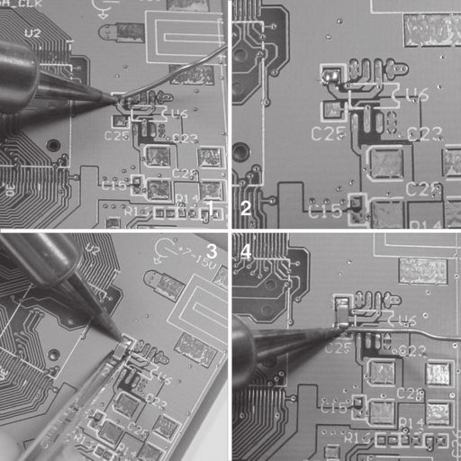
Figure B-1: (1) Apply a touch of solder to one of the target component’s pads. In this case, the target component is C25. (2) Picture of the solder blob after application. (3) Use tweezers to align the target component and then apply heat with a soldering iron until the initial solder blob has flowed around the component’s leads. (4) Solder the remaining component pads.
First, place a blob of solder on one of the component’s pads, then place and align the component over its pads using a pair of tweezers. Once you feel comfortable with the component’s placement, apply heat to the blob of solder until it melts and the component sinks into place on its pads. Keep applying the heat while you adjust the alignment of the component. Remove the heat, and wait for the solder to cool down and solidify. Double-check the alignment of the component, and then solder the rest of the component’s contacts to the board. If the first solder joint looks dull or weak, reheat it with a touch more solder once all the other pins have been soldered down (see Figure B-1). This technique works for components with two or three pins, and for multi-pin components with a wide pitch, such as the 50-mil pitch small outline IC packaged devices.
The most difficult situation you may encounter when soldering down these components occurs when one or more of the component leads are attached to a large area of copper, such as a power plane. In this case, a large amount of heat must be applied to the PCB pad before the solder will wet and adhere to the circuit board. Beware when this happens, as the solder will oxidize and ball up, and make poor electrical contact with the board. Add a touch of solder flux if this situation occurs to help enhance the wetting action of the molten solder.
Tip

A “dry” soldering iron tip will have trouble heating large patches of copper, or pads that are connected to power planes. One way to increase the rate of heat transfer from the soldering iron is to start the iron out with a blob of molten solder on the tip, and touch the iron to the board through the molten solder blob. This blob will spread out and heat the board locally, and will establish a good thermal connection that more effectively transfers heat. This will ultimately lead to a better solder connection once more solder is added.
Technique for Complex Components
Most integrated semiconductor components today are available in some kind of a fine-pitch surface mount package. This kind of packaging can be intimidating at first, but a little bit of practice with a few simple techniques and tips is all it takes to attach these parts with a high degree of confidence. The process of attaching a fine-pitch surface mount component is very similar to that of attaching a simple surface mount component, and it should take no more than a few minutes for a typical mid-sized surface mount package.
The first step is to tack the component on the circuit board by soldering down only two corner pins on the chip. If the alignment is not correct on your first try, it is easy to correct by just heating one of the two corners while pushing the chip in the desired direction for alignment (see Figure B-2). Be very mindful of the accuracy of this alignment: a misaligned chip will lead to no end of frustration while trying to solder the chip down.
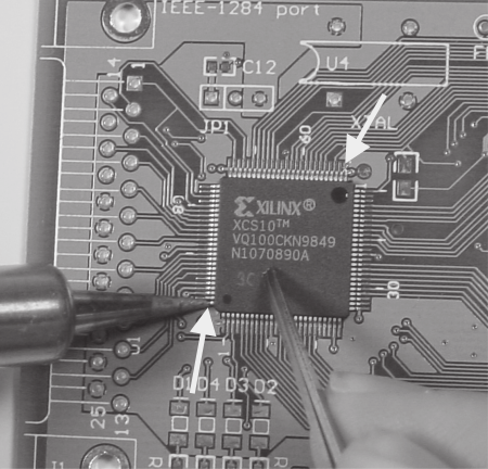
Figure B-2: First, solder down one pin on each of two opposite corners of a chip. The arrows on this diagram indicate the corners used in this example.
The next step is to apply a thin film of solder flux around the chip. This will enhance the wetting action of the solder on the chip pins and cause the solder to wick onto the component pads, instead of in between the leads, which would cause a short (see Figure B-3).
Tip

When laying out a board, use extra-long pads for fine-pitched surface mount components. The extra length will make hand-soldering easier, though it will also make routing a little bit more difficult and cause the board size to grow slightly. The extra pad length acts to wick away excess solder from the chip leads, thus making solder bridges less likely.
Once all of the leads have been uniformly coated with the soldering flux, load the tip of a soldering iron with a tiny ball of solder, and press this ball up against the unsoldered leads. The ball of solder will wick into the space underneath and around the component leads. Repeat this process until all of the leads have been coated with solder. Do not worry at this point if excess solder bridges multiple pins. Once you are finished soldering all the pins, use a copper desoldering braid (solder-wick) to remove any solder bridges, as shown in Figure B-4.
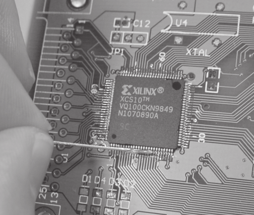
Figure B-3: Apply a thin film of solder flux to the pins around the chip. In this illustration, a paste flux is being applied using a scrap piece of wire that is frequently dipped in the flux container.
You are almost done. Finally, make sure that all the pins are firmly soldered down. It is difficult to do this inspection visually without a microscope. Instead, pull on the pins with a needle or the tips of a tweezer, dragging the tweezer along the pins as shown in Figure B-5 using a firm, steady motion. Pins that are not soldered in place will move slightly. If they do, repair them by pushing them back into place, and applying a touch of solder to the pin.
Caution

Always check for power shorts after soldering a circuit board. Some solder bridges can be microscopic dendrites, and some solder bridges will form behind the pins underneath the chip. Check for power shorts using a multimeter set to measure resistance. Do not use the audible continuity mode, as large, high speed computer boards usually have a low (few ohms) resistance between power rails, which is low enough to register a short on many continuity meters. Also, when measuring the resistance between power lines, wait a second or two for the measurement to settle. The initial resistance between power rails wil be very low while the large capacitors that sit on the power lines charge up.
Once your component has been soldered down, clean up the excess flux using a mild solvent, such as Isopropyl alcohol, and a cotton swab as shown in Figure B-6. Clean-up is important because it makes visual inspection easier, and it also makes it easier to probe the chip pins during debugging. It is also important because many fluxes tend to crust over and trap contaminants with age, hampering future repairs.
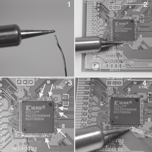
Figure B-4: (1) melt a small amount of solder onto the tip of a hot iron. (2) Transfer this solder onto the pins of the component. Repeat steps (1) and (2) until all pins are soldered. (3) Solder bridges, indicated with arrows, will have formed across many pins. (4) Remove the solder bridges using a piece of copper desoldering braid.
Technique for Removing Components
There are many techniques for removing surface mount components, and many of them require special tools, such as tong-style soldering irons or hot air guns. Tong-style soldering irons are good for removing smaller surface mount components, especially on boards that are densely packed. They are fairly quick and efficient, and a proper tong-style soldering iron will leave the pins of the component in relatively good condition. However, they are also fairly expensive, and a bit of practice is needed in order to figure out the right timing and pressure to use when removing a chip.
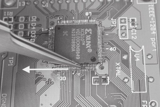
Figure B-5: Stroke the pins along the side of the chip using a pair of tweezers or a needle using a firm, steady force. Pins that are not soldered well will bend slightly. The arrow indicates the direction of motion.
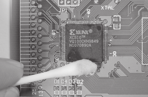
Figure B-6: Clean up the flux residue using a cotton swab dipped in a mild solvent.
An easier and cheaper solution is to use a heat gun, like the ones sold in hardware stores for removing linoleum floor tiles. The heat gun will heat the entire region of a board, and components will float off their pads with minimal damage to their leads. The downside of this technique is that it is not very precise, so it is not an ideal solution for removing chips on boards that are going to be used again. As a result, heat guns are most effective for salvaging good chips from broken boards. The other problem with using heat guns is that the heat can warp boards or cause destructive failures in chips that have absorbed moisture into their packages. This failure mode, called “popcorning,” happens when moisture trapped inside a chip boils but cannot escape, causing a pressure buildup that culminates in a destructive release event. Chips and boards operating in a humid environment or that have been washed in water should be baked in an oven at around 200 to 250°F for a few hours before desoldering with a heat gun.
Another option that is particularly appealing for hobbyists is to re-alloy the solder joint so that it melts at a very low temperature, below 300°F. A company called Chip Quik (www.chipquikinc.com) holds the patent on this technique, and removal kits can be purchased from many vendors, including Jameco (order number 141305). This technique is appealing because it requires no special equipment, and it is easy and fairly safe, as shown in Figure B-7.
To do so, first coat the chip pins with soldering flux, then melt the chip removal alloy onto the pins of the component to be removed. This will create a large bead of low melting temperature alloy all around the chip. Next, heat the entire bead by dragging the tip of the soldering iron through the bead. The stored heat in the chip and the alloy will keep it molten long enough for the whole chip to be easily slid off its pads. Finally, clean up the low melting temperature alloy by heating it with a soldering iron and then wiping it away with a cotton swab. The alloy will wipe off fairly easily from both the board and the chip.
This re-alloying technique preserves the integrity of the removed chip’s pins as well as the pads on the circuit board. The downside of this technique is that cleaning up the alloy can be a bit messy, and tiny particles of alloy can get caught between the pins of neighboring chips. (Caution while cleaning up will prevent this problem.) The other downside is that removing chips consumes the removal alloy, so removing large numbers of chips with this alloy can become expensive in the long run. Fortunately, chip removal is a fairly rare occurrence for most hobbyists.
The “ball grid array” (BGA) package is a type of surface mount package that is becoming increasing popular due to its high electrical performance and density. These packages are attached to a board through a large array of solder bal s underneath the package. Clearly, this kind of package cannot be soldered using a conventional soldering iron. In addition, BGA packages are very difficult to inspect because most of the solder connections are buried deep below the package. The only viable method for attaching these components is to use an oven that heats the whole board and the component to the point where all the solder balls melt. Typically, the alignment of these BGA packages is accomplished with the aid of a machine of some kind, and the inspection of these BGA packages is accomplished with either X-rays or ultrasonic imaging.
The equipment required to install these kinds of packages is very expensive, so the best way for a hobbyist to install a BGA packaged device is to pay a professional assembly house to do it. Companies such as Naprotek (www.naprotek.com) that specialize in quick-turn, low volume prototyping will install a BGA packaged device for a fairly reasonable fee. When getting a BGA installed, always ask for a copy of the inspection photo for the part; the peace of mind brought by the photo is worth the extra cost. BGA parts can also be removed and reballed, although this process can be much more pricey than the attachment process.
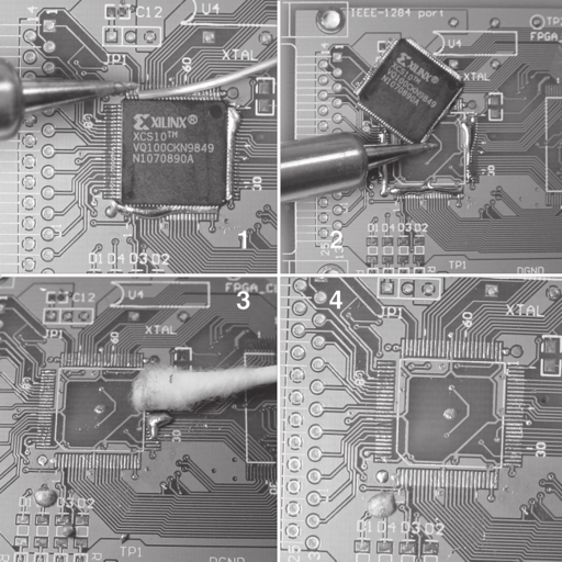
Figure B-7: Removing a chip by real oying the solder joint. (Prepare the chip pins with soldering flux before starting this process.) (1) Melt the realloying compound onto all of the chip pins. The realloying compound comes in wire form. (2) Heat the blobs of metal around the chip by dragging a soldering iron through the metal. Al the realloyed solder will become molten, at which point the chip can be pushed off its pads. (3) Clean up the realloying compound from the board and the chip by heating it and wiping it away with a cotton swab. (4) The result, a clean chip removal.