8: Designing an Anode Tank Circuit
This topic is covered in full detail in one of my other books, RF Design Basics
(RSGB, 2007) so I will just cover the basic parts here. If you wish to have a more in-depth explanation the book mentioned is a good reference source. It also contains full tables for different loaded Q networks, which save a lot of effort to derive the correct values for the components.
The most commonly used anode matching network used in HF linear amplifiers is known as the pi network and a typical type is shown in Fig 8.1.
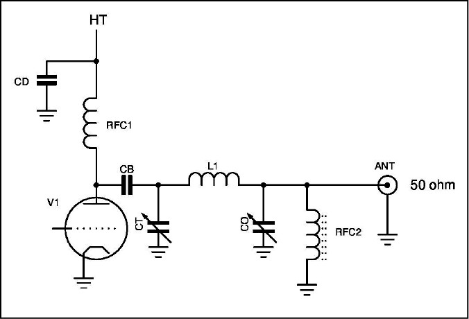
Fig 8.1: The pi network.
The network consists of just three components that perform the impedance transformation from the valve anode to the load. These are two tuning capacitors shown as CT and CO and the series inductor L1. The rest of the components are required to ensure correct operation of the valve and for other purposes. The anode DC feed is via the inductor RFC1 and is decoupled to RF ground by CD. Capacitor CB is simply a DC block to prevent the high voltage appearing across the antenna terminal and it serves no function in the matching network. Generally, this capacitor is chosen to have a low reactance at the operating frequency. Similarly, RFC2 is a safety device to short out the anode high voltage supply should CB fail short circuit. The normal anode parasitic APC is not included as it has no effect on the matching network.
To design an anode network we need to have certain facts to hand. The most important details are the required anode load resistance, the required loaded Q value the network must work at, and the valve anode to ground capacity. Without these values we cannot begin.
We have some freedom of choice with the loaded Q, but it can impact on whether a solution is possible or not with the selected valve and operating conditions chosen. The anode load resistance will often be quoted by the manufacturer, but in some cases it isn’t given. We will select the 811 valve and choose to have three valves in parallel to attain the wanted output power.
In the older data sheets for the 811 valve operation in Class B isn’t given for RF applications, but a figure is given for two valves in push-pull for audio amplifiers. The anode load quoted for this application is 12,400Ω anode-anode. Hence, each anode represents half this value, 6200Ω. This is for an anode supply of 1500V and an average anode current of 313mA for two valves. The average anode current per valve is hence half this figure.
As a check to see if these numbers stack up, we can do a quick check. The anode supply of 1.5kV, when multiplied by 313mA, gives an input power of 470W and the quoted output power is 340W. The efficiency is hence (340 / 470) = 72%, which for a Class B audio amplifier is reasonable.
So we know the values are about right and we can now proceed.
Paralleling three valves each with an anode load of 6200Ω gives an equivalent anode load of 2066Ω, which we can round down to 2kΩ. The anode current will be (313 / 2) x 3 = 470mA. Each valve’s idle current is given as 32mA. This, however, needs a –4.5V grid bias at this higher anode voltage. (If we used a lower anode supply of 1250V the normal zero bias would cater for the idle current setting.) To convert the negative grid voltage to the cathode voltage we simply invert the sign, so we need to lift the cathode above ground by +4.5V to get the correct idle current. Hence, the idle current with three valves will be about 100mA.
The loaded Q we will choose is 12, as this is a good compromise.
We now need to know the anode output capacitance and the data sheet gives a value of 5.6pF for a single valve. Allowing for some stray capacity we will assume each valve looks like a 7pF shunt capacitance to the anode network. So with three valves the value is 21pF.
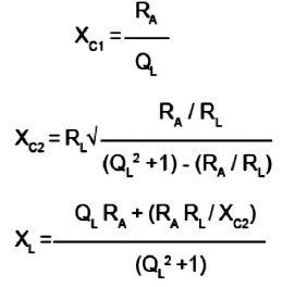
The anode tuning capacitor value required is determined by the loaded Q and the anode load value. This gives us the reactance of the anode tuning capacitance CT. In the standard formula for the pi network this is normally denoted C1. The standard formulas are shown below when RA is much larger than RL.
XC1 = Ra / QL
Note: Only C1 determines the loaded Q and no other component has an effect. This gives a value of 172Ω at the operating frequency.
Now we convert the reactance to the actual capacitor value required at the operating frequency. We will design for the 80m band at first, you will see the wisdom in this later.
At 3.5MHz we require an anode tuning capacitor of 272pF. The anode capacitance is already 21pF, so we need a tuning capacitor of (272 – 21) = 251pF. This value should ideally be with the capacitor at about half-meshed. So in reality we need about a 500pF total value. This is a large capacitor, so we elect to use something smaller and make up the difference with a fixed capacitor.
Suppose we have a 150pF maximum tuning capacitor with wide spaced plates that would safely handle the envisaged anode voltage swing. We can estimate that the peak anode voltage swing will be about twice the DC supply, so a 3kV minimum is the lowest we can use and a 5kV type would be a better choice. The anode tuning capacitor is hence a 150pF set to about half mesh and the rest is a fixed capacitor wired in parallel. Half of 150pF is 75pF and the fixed capacitor needs to be 175pF. The closest standard capacitor is 180pF and this will suffice.
Now we calculate the value of the loading capacitor C2 using the formula to match to the 50Ω output load. This gives a value of 1474pF. The RF voltage at the output is much lower than the anode voltage as the transformation from 2kΩ to 50Ω is a ratio of 40:1. This could use a multiple-gang broadcast type with about 365pF per section and a voltage rating of 350V AC. (If the RF voltage is 150V RMS the power in 50Ω is 450W.)
A three-section type would be a total of ~1100pF. But the required value is the fully loaded value and this should occur with the capacitor almost fully unmeshed. So the additional fixed capacitor required is greater. We estimate that when correctly loaded the variable capacitor is 3/4 unmeshed and it will have a value of about 275pF. Hence, the fixed capacitor required is (1474 – 275) = 1199pF and a 1200pF fixed capacitor will suffice.
The final component to be calculated is the series inductance and this requires a value of 8.25µH.
Adding Additional Bands
If we also wish to cater for 40m, a simple way is to halve all the values just calculated to find the correct values for 7MHz.
The value of C1 required for 7MHz is 136pF total. We subtract the 21pF anode capacitance of the valves to obtain the tuning capacitor value of 115pF and our 150pF maximum will fit nicely without any extra fixed capacitor needed. The loading capacitor needed is (1474 / 2) = 737pF total and as the three-gang capacitor is 1100pF when fully meshed it would only be 67% meshed at this setting. So we need a fixed capacitor to bring the three-gang capacitor closer to 3/4 unmeshed. A fixed value of about 470pF would work well.
The inductor is simply (8.25 / 2) = 4.125µH.
The other bands that are harmonically related such as 14, 21 and 28MHz are calculated in the same manner by dividing the values by the correct factor.
The two highest bands are where we may have a problem as the anode capacitance is a fixed value of 21pF and we cannot change that.
At 28MHz with a loaded Q of 12, the total anode capacitance needs to be 34pF and so the tuning capacitor only needs to be 13pF to resonate the circuit. With the 150pF total capacitor chosen the capacitor is almost totally unmeshed, so it isn’t likely to work. This is because its minimum is not 0pF but usually about 5 to 10% of the maximum value. If the minimum is 10% it cannot be reduced below 15pF in value with the plates completely unmeshed.
There are two solutions to this problem. One is to switch a suitable value series capacitor into circuit between the anode and the tuning capacitor or to increase the loaded Q. The higher the loaded Q the lower the reactance of C1 needs to be. A low reactance is a higher value of capacitor.
If the loaded Q is raised to 16 the value required for C1 increases to 45pF total and when the anode capacitance is subtracted it leaves a value of 24pF, which is more practical, but still too low a value. If the loaded Q is increased to 18, C1 becomes 51pF total and C1 needs to be (51 – 21) = 30pF and for a loaded Q of 20 it is 56pF total and a capacitor value of 35pF.
This is a common problem when the anode capacitance is high and most HF amplifiers do not in fact use a constant loaded Q value for all bands for this reason. As the frequency increases the loaded Q normally has to be increased to keep the anode tuning capacitor within practical values.
In a case such as this we cannot keep pushing up the loaded Q because the anode network loss rises with increased loaded Q. A practical solution would be to use a smaller value anode tuning capacitor and to add fixed value padding capacitors for the lower frequency bands to bring the lower value capacitor to about mid-value. Alternatively, we could make the capacitor C1 from a dual-gang type and to switch out half of it for the higher bands. None of these are ideal, as extra switching is required.
However, a high loaded Q does not mean the loss will be very high and lower the output power by any considerable amount. At the higher frequency it is simpler to make high Q inductors and the loss is predominantly defined by the inductor unloaded Q. An 80m tank coil with many turns of small diameter wire will have a far lower unloaded Q than a 10m inductor wound from substantial gauge wire or copper tube. This inductor is a small number of turns and unloaded Q values of 450 or more are achievable. The difference between an unloaded Q of 450 and one of only 100 is about 5% in power loss in a practical amplifier. This is 0.25dB and isn’t anything to get excited about. The Q of a good quality anode tuning capacitor is at least 3000 and the loading capacitor is often about half this figure. The pi tank series inductor, if wound correctly, contributes as little as 2 to 5% loss.
Anode DC feed choke
So far no mention has been made of the anode RF choke that supplies the anode current. The item that normally contributes the greatest loss in a pi network is the anode DC feed choke, which accounts for about 30% of the total losses. This is because it is very difficult to make a multi-band choke, wound with small diameter wire, with a good Q.
Normally when calculating the pi network components the effect of the anode choke is ignored. However, its inclusion into the network can have a dramatic effect on the operation of the network.
The general rule of thumb, when a choke needs to be connected in parallel in a circuit, is to assess how much it disturbs the working of the network. If the reactance of the choke is infinite it has zero effect. But in a practical circuit we cannot make a choke with an infinite reactance. The assumption made is that if the reactance of the choke is 10 times higher than the portion of the network it is attached to the disturbance it makes is insignificant and can usually be ignored. In our example it is connected to a point in the network that at resonance behaves like a 2kΩ resistance. Hence, the choke reactance needs to be at least 20kΩ. At 3.5MHz this is a value of 909µH. This value is impractical and it would be very difficult to wind such a choke and guarantee no spurious resonant frequencies.
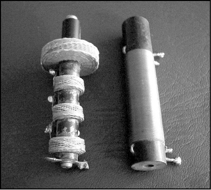
Two typical anode chokes; left: for a multi-band HF amplifier, right: for a single-band design.
The way to avoid this problem is to use the shunt capacitance between the anode and ground to resonate a lower value inductor to the operating frequency. If the correct value inductor is connected across the anode to ground it would behave like a very high value resistor because of its dynamic resistance (RD). Eimac covers this aspect in an engineering bulletin. A chart showing the optimum resonant frequency is shown in Fig 8.2.
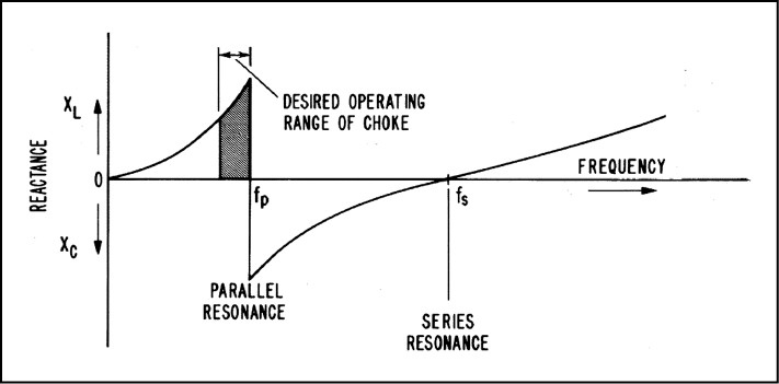
Fig 8.2: Optimum RF choke resonant frequency (from ‘Care and Feeding of Power Grid Tubes’, Eimac).
Obtaining the correct band of parallel resonance can be fraught with problems. This often causes an apparently well designed anode choke to burn up. The stress on the anode choke is considerable. Not only does it have to carry the fairly high dc load to feed the anode but at tank circuit resonance the RF voltage impressed across the choke approaches twice the anode supply voltage. If the reactance or RD is not high enough then a large AC signal can flow to ground in the choke. It is decoupled at the supply end so it is effective grounded.
In our example amplifier using a 1.5kV anode supply the peak-peak anode voltage swing will be about 2.5kV at maximum RF output. If the choke reactance or the RD is 10kΩ, the peak RF current flowing to ground is 250mA. This is effectively lost power. If de-tuning the anode capacitor a small amount causes the choke RD to drop to 5kΩ the RF current doubles. This extra current, plus the higher anode DC current which will occur when the anode is de-tuned, can put too much stress on the choke and it will object by heating up.
A Better Anode Feed Choke Method
The shunt feeding of the anode supply has always been a difficult problem and there must be a better way of tackling this portion of the anode matching network. After much thinking a new method was evolved.
The real problem is that the spurious resonant frequencies are very hard to control or predict if the inductor value is large. But if the inductor didn’t need to be such a large value a better chance exists of keeping these gremlins in check.
The solution is actually very simple. If the pi tank network is re-arranged slightly a workable solution is easy to incorporate. The first step is shown in Fig 8.3.
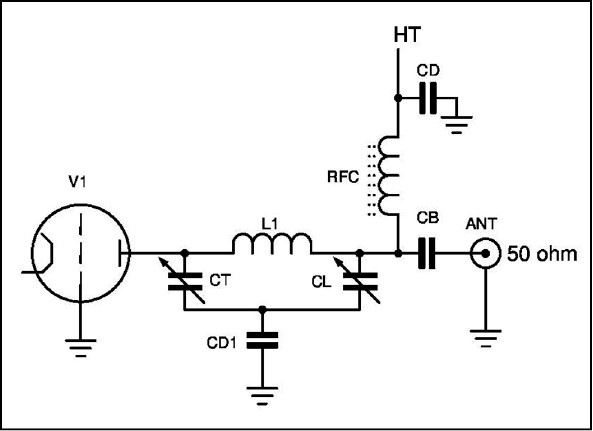
Fig 8.3: Modified anode DC feed method.
In this method the anode blocking capacitor is moved from the anode to the output connector. The choke now feeds the high voltage DC into the tank circuit at the 50Ω point. Consequently, it only needs to have a reactance of ~500Ω at the lowest operating frequency. This gives an answer of 22.7µH and a choke larger than this would suffice. As the RF voltage is much less than when at the anode, winding a suitable choke is much simpler. The one disadvantage of this method is that the tuning and loading capacitors now have to float at the anode DC supply level. This is not really a problem in practice and the use of insulated shafts and shaft couplers readily supplies the required isolation.
The output DC blocking capacitor needs to be a larger value than for the anode position, but again this isn’t a problem. The RF output current, although higher, is not excessive and normal high voltage capacitors are available. For an output power of 450W in 50Ω the RMS current is 3A.
The output can still suffer from a DC blocking capacitor failure and a shunt RF choke across the output would be required to blow the anode supply fuse should this occur. A further tweak was suggested by my Chief Engineer at the time, Greg Smith, now ZL3IX, and this is the final answer. The final circuit is shown in Fig 8.4, which is quite an elegant and clever bit of design.
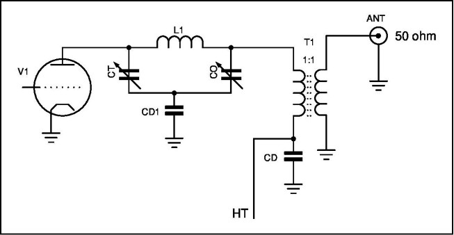
Fig 8.4: Isolated anode DC feed method.
The addition of a 1:1 RF transformer solves the potential blocking capacitor failure mode and allows the elimination of the DC feed choke at one fell swoop. Transformer T1 is wound on a ferrite core with small diameter Teflon coax cable and needs to have sufficient inductance to cater for the lowest frequency.
Anti Parasitic Chokes
This topic has already been touched on in an early part of the book. There is a lot of myth and urban legend on this topic. A lot of this is attributable to one person who seems to have a fixation with the topic. I won’t mention the name or callsign, but those who have followed this saga know who I am alluding to!
The statements made about APCs that they should be wound from resistance wire or some other lossy material, such as stainless steel, are completely incorrect. The APC is inserted to form a parallel trap at the offending frequency so that it becomes parallel resonant with the valve or circuit capacitance. Most parasitic oscillations occur in the VHF region, so the inductor value needs to suit this operating range. In most cases a few turns of copper wire are used formed on a 2W carbon composition resistor and connected to the resistor lead out wires. The resistor value is very low, typically about 22 to 56Ω seems to work in 99% of cases.
The inductor will have a reasonable Q and hence will have a narrow range where it is effective with the anode capacitance. The purpose of the low value resistor is to flatten the frequency response so it covers a much greater bandwidth. It also serves as a dummy load to any parasitic power.
The effect the APC has on the normal anode tank circuit is very small and as the anode and loading capacitors have ample range they can easily compensate for the addition of this small extra inductor in series with the anode terminal.
The requirement to only use a lossy wire is rubbish.
The copper wire when formed into an inductor and resonated by the stray capacity will have a Q of perhaps 100 or so. It will exhibit a dynamic resistance of about 5kΩ or possibly higher. But the connection of the low value resistor across the inductor completely destroys any Q it had. The Q drops to 1 or even below, which is exactly what we need to form an effective APC. The person who persists with this argument states that although you use nichrome wire or stainless steel strip to wind the inductor, it still needs the resistor. This shows that the resistance wire isn’t being as effective as they think it would. If the resistance wire was doing what they claim it does, the resistor would not be needed.
In many parasitic oscillation cases the inclusion of a 1/2W carbon composition resistor in series with a grid pin on the valve solves the problem. This has no significant inductance but it stops the oscillation. In most cases the resistor does not need to be a very high value, 10Ω to 47Ω is often more than enough.

