4: The Class A Amplifier
The simplest type of amplifier is one that operates in Class A. Not only is it
simple to design but it also has the best linearity of all the various types. However, it is not the most efficient type and is limited to fairly low power applications, as the power dissipation is high. It is commonly used in audio small signal stages, such as microphone amplifiers, as it also is a low noise type when triode valves are used. In RF applications it is used where linearity is critical in low power stages of transmitters and receivers.
The gain that a Class A amplifier can achieve is surprisingly high for such a simple circuit. Voltage gains of 50 to 100 are relatively easy to achieve and it is easy to cascade two or more stages to get even higher gain. Although the voltage gain is high the power gain is somewhat limited.
The basic circuit of a simple triode valve amplifier is shown in Fig 4.1.
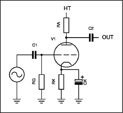
Fig 4.1: Class A amplifier schematic.
To calculate the various component values for a Class A amplifier, first we have to choose a suitable valve. For small signal amplifiers there is a host of different valves suitable, but some are more commonly available then others. A good choice would be the ECC82 / 12AT7 or, for higher gain, the ECC83 / 12AX7. These are dual triodes, so there are two identical triodes in one envelope, which saves space. Although each half of the valve is separate they share a common set of pins for the heaters. We will choose a valve with a transconductance of about 2 to 3mA/V, which can safely handle up to 250V anode voltage.
The common circuit for a Class A amplifier is a grounded cathode topology which is an inverting amplifier. The anode voltage waveform is 180º out of phase with the input signal. In the Class A small signal amplifier the normal rule for biasing is known as the ‘50-50’ rule, which states that ‘the anode voltage is 50% of the supply rail and the anode current is 50% of the valve maximum current’. This is illustrated in Fig 4.2. The typical triode characteristics shows that at very low and very high anode current the curve deviates from a straight line. To ensure that the distortion is low it is necessary to keep out of these regions.
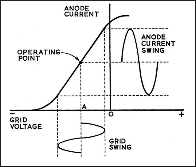
Fig 4.2: Biasing diagram for Class A operation.
By using the 50-50 rule we set the anode voltage to half the supply voltage and the anode current is midway between zero current and the safe maximum for the valve chosen. In many cases the anode current will be only a few mA. There is a wide range of choices for the anode supply voltage and as the valve chosen can safely tolerate up to 250V anything up to this voltage is acceptable. Suppose we have a +150V supply rail present, then it makes the design easier to use this voltage.
Straight away we have fixed the anode voltage to be half of 150V, so the quiescent bias point is +75V above ground. The anode current can be anything up to about 5mA as this fits within the manufacturer’s range of working conditions. We will select a quiescent anode current of 2.5mA, as this is midway between the minimum and maximum.
To calculate the anode load resistor RA we use Ohm’s law: R = V / I
We need a resistor that will drop the 150V supply rail to 75V when a current of 2.5mA flows. Hence, RA = (75V / 2.5mA) gives an answer of 30kΩ. This is not a standard E12 resistor value, the nearest values are 27kΩ and 33kΩ and we will initially select the 33kΩ option. We now check what the anode voltage is for this resistor.
Using Ohm’s law (V = I x R), for a 2.5mA current and a 33kΩ resistor, V = 82.5V drop. This places the quiescent anode voltage at (150 – 82.5) = 67.5V, which is normally close enough. If we wanted exactly the mid-rail voltage of 75V we could use 2 x 15kΩ in series.
If we selected the 27kΩ resistor the voltage drop would be 67.5V and the quiescent anode voltage is +82.5V. This is also close to the required value. A simple method of getting the voltage to exactly half-rail is to change the quiescent anode current a little. For the 33kΩ resistor we would need a quiescent anode current of 2.27mA and for the 27kΩ resistor it is 2.77mA. Since both of these options are a small change we will ignore the error at present.
Studying the manufacturer’s data sheet we now find the correct bias voltage on the control grid by reading off the constant current curves. We find that for the required quiescent anode current and voltage we need –2V grid-cathode voltage. Since the anode current also flows via the cathode resistor RK to ground we need to raise the cathode voltage +2V above ground when the current of 2.5mA flows. Using Ohm’s law we find: RK = (2V / 2.5mA) gives us a value of 800Ω and the closest E12 value is 820Ω.
To determine the value of CK we need to calculate the capacitor value that is at least ten-times lower in reactance compared to RK. It needs to be less than 82Ω at the lowest frequency encountered. If this is a microphone amplifier for a transmitter, normally we need not go lower than about 300Hz. A 10µF capacitor at 300Hz has a reactance of 53Ω and this would be suitable. If the amplifier were for a hi-fi amplifier then a larger value would be needed to cover down to about 20Hz, a 100µF would be suitable.
The input and output coupling capacitors are chosen to be a low reactance at the operating frequency. For audio amplifiers a value of 100nF is usually suitable as the impedance of the input and output are both high. The coupling capacitor connected to the anode needs to have a suitable voltage rating, a 250V capacitor would be suitable. The input capacitor needs very little voltage rating and a 50V type would be suitable.
All the component values have been determined, except the input grid resistor RG. If the microphone were a high impedance type, a suitable resistor would be greater than twice the microphone impedance. If the microphone is a 47kΩ type a resistor greater than 100kΩ would be suitable. We will choose a 1MΩ. (Some microphones are a bit fussy if not used with the correct impedance load: it may be better to choose a 47kΩ resistor.)
Now that all the values are determined, how much voltage gain can we expect?
If when we check the DC conditions on the anode to ground we find that the voltage is not at the midway point, a small adjustment to the cathode resistor RK will bring the voltage to the required value. This could be done with a variable resistor in the cathode return. If the cathode resistor is made up from a 560Ω fixed resistor and a 500Ω variable resistor this gives us the ability to trim the anode voltage to the exact value required. However, in simple amplifiers it is not normally necessary to go to such lengths. A DC instrumentation amplifier would probably require this fine adjustment.
Voltage Gain
To a first approximation the voltage gain is (RA x gm) this gives a value of (33 x 103) x (2.5 x 10–3). Since the 103 and 10–3 terms cancel, the answer is (33 x 2.5) = 82.5.
Assume that the maximum input signal is 100mV RMS. The peak-peak input voltage will be 282.8mV (0.2828V). With a voltage gain of 82.5, the anode voltage swing will be (0.2828 x 82.5). This is a peak-peak voltage of 23.33V, in RMS values it is 8.25V.
The anode voltage will move up and down, centred on the nominal +75V quiescent point, and reach a maximum of (23.33 / 2) + 75 = 86.66V and a minimum of 75 – (23.33 / 2) = 63.33V.
Since the total anode swing is much less than the nominal +75V bias point the swing is small in percentage terms and the linearity will be very good.
Now we ask the question, how much input signal can the amplifier tolerate before it becomes distorted?
Suppose the input signal is now raised to 0.2V RMS. This is a peak-peak input swing of 0.565V. The anode current will change by ±(0.565 x 2.5) = 1.414mA either side of the quiescent current of 2.5mA. This gives the minimum and maximum anode currents of 1.08mA and 3.53mA. The anode voltage swing will be ~47V either side of the quiescent point of 75V.
It will swing down to +28V and up to +122V. Since the supply rail is +150V, it is getting close to this voltage. Similarly, a valve needs a certain minimum anode-cathode voltage to work correctly. The swing developed is about the maximum that we can realistically expect to be acceptable.
Knowing the voltage gain is 82.5, we could also find the approxi-mate output voltage swing by simply multiplying the input voltage peak-peak value by 82.5. Hence (82.5 x 0.565) = 46.66V.
For a greater output voltage swing it is better to use a higher supply voltage and a higher anode load resistor to achieve the same quiescent bias point of 2.5mA. If a 250V supply were available, the output swing can be greater for the same input signal. Hence, the potential output voltage swing, and hence the voltage gain, is directly related to the value of RA.
If we calculate the new value of RA for a supply voltage of 250V, with the new anode quiescent voltage of 125V it requires a resistor of 50kΩ.
Very often a manufacturer will give details of component values and an application circuit. One example is shown in Fig 4.3 above, for the ECC83 / 12AX7 valve.
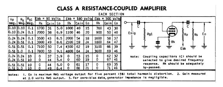
Fig 4.3: Component values and application circuit for the ECC83 / 12AX7 valve (from General Electric data sheet).
Cascaded Stages
Where we require more gain than a single stage can achieve we can achieve sizeable gain values by connecting two or more stages in series. If each stage has a nominal gain of 30, two stages will give a total voltage gain of 900. Three stages would achieve a total voltage gain of 27,000. An example of a simple cascaded amplifier is shown in Fig 4.4.
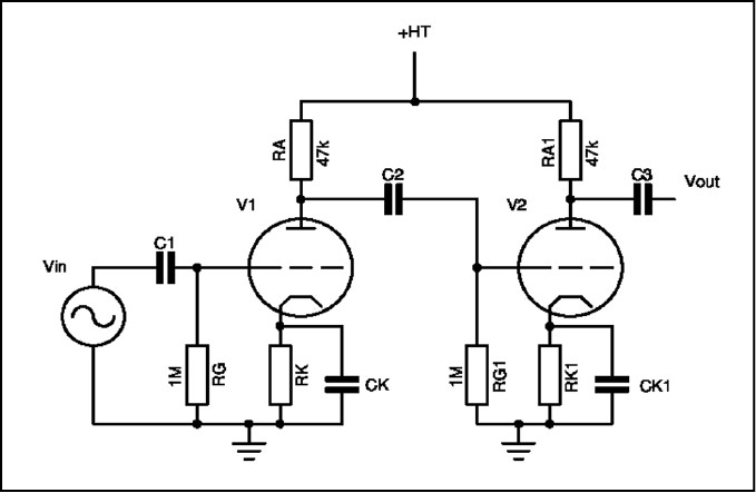
Fig 4.4: Two cascaded triode amplifier stages.
Note that the value of the grid resistor in the second stage has a bearing on the anode voltage swing of the first stage. If the value of this grid resistor is too low then the network acts as a potential divider. If the grid resistor of the second stage is the same value as RA the voltage across the grid of the second stage is 50% of the output voltage of V1. Generally, it is necessary to use a much greater value for RG1 to allow the full voltage swing to occur.
A potential problem with this type of ‘resistance coupled’ amplifier is the leakage current in the coupling capacitor between the anode of the first stage and the grid of the second stage. If this capacitor has a high leakage current it will force the grid of V2 to rise above the required bias point. This is often a problem in old equipment. If the leakage current is only 1µA, the voltage developed across RG1 is +1V. If the grid needs to be biased to –2V this upsets the correct biasing point. Hence, these capacitors need to be chosen with care.
Pentode Amplifiers
The simple triode amplifier is a bit limited in the transconductance values that can be achieved. Where greater stage gains are required the use of a pentode valve is often a good option. The pentode valve is similar to a tetrode and has an extra grid structure, the screen grid or Grid-2. The increase in the transconductance compared to an equivalent triode can be as high as five times. The anode current variation it can generate is much greater for the same input signal. In simple terms, it has more potential voltage gain.
Many of the common audio amplifier valves are made as triode-pentode or triode-tetrode types, with the two valves in one envelope. (One such type is the ECL-82, which is a popular device for driving low power speakers. This is a triode and a beam-tetrode in a common envelope.) Not only has the pentode more voltage gain, it has a greater current gain, so it is capable of supplying a reasonable power. Pentodes and tetrodes are noisier valves than triodes, so the first stage is usually the triode section and the pentode is used to drive the loudspeaker via an impedance matching transformer.
Some of the classic audio amplifier pentode valves are popular as microphone, guitar or phono input stages as the gain is considerable and they can swing the anode voltage over quite a large range. A voltage gain of over 100 is normally possible. One popular valve is the EF86 / 6F22, which is a low current pentode that can provide a stage gain of 150 from a 250V supply (Fig 4.5).
The EF86 is a low current valve and typically it will be operated from a 300V to 450V supply and draw ~1mA quiescent current. Anode load resistance values are found in the same way as a triode valve, by consulting the manufacturer’s data sheet to obtain the gm value.
The screen grid (g2) will require a dropper resistor from the high voltage supply rail and a suitable decoupling capacitor to prevent variations of the voltage. Often this capacitor can be a low value as the dropper resistor is normally a high value. This capacitor and CD need to be adequately rated for the voltage.
The third grid (suppressor grid) needs to be connected either directly to ground or to the cathode. In some valves this is an internal connection. The EF86 grid-3 is brought out to the base pins for the user to connect. In addition the EF86 also has internal electrostatic shields or screens to reduce hum pick-up and these two pins also need to be grounded. The internal shielding often means that a screening can over the valve is not necessary. The EF86 uses the standard B9A valve base and requires a 6.3V heater supply at 200mA: see Table 4.1.
Pin No. | Designation | Function |
1 | g2 | Screen Grid |
2 | s | Internal Shield |
3 | k | Cathode |
4 | h | Heater |
5 | h | Heater |
6 | a | Anode |
7 | s | Internal Shield |
8 | g3 | Suppressor Grid |
9 | g1 | Control Grid |
Table 4.1: Valve pin connections of the EF86 pentode.
Using the component values of Fig 4.5 an output voltage swing of about 100V peak-peak is possible before the distortion becomes unacceptable.
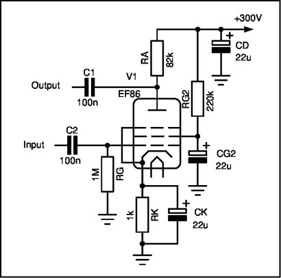
Fig 4.5: Typical high gain audio amplifier using the EF86 pentode.
Hum prevention
In common with all high gain stages, the prevention of hum and other extraneous signals is largely a function of layout and grounding. The heater wiring is a potential source of hum so the routing of these wires is important. Often the best method is to twist the two wires tightly together and not to ground the heater secondary winding.
Another source of hum is ripple on the power supply rail. To reduce this it is common to supply this from a higher voltage via a suitable dropper resistor and a large value decoupling capacitor to form a RC low pass filter. In Fig 4.5 the decoupling capacitor CD performs this function. For operation from a 350V supply, a dropper resistor of about 10 to 33kΩ can be used.
RF Class A amplifiers
For low power stages in a transmitter where linearity is critical the Class A stage is a good choice. The anode load resistor is replaced with a resonant parallel tuned ‘tank circuit’ tuned to the required frequency.
The dynamic resistance of the anode load is chosen to be high by selecting the value of inductor and capacitor with cognisance of the inductor unloaded Q. Very often the loaded Q is too high and this causes a narrow band over which the amplifier will deliver power. To correct this a damping resistor can be shunted across the tuned circuit to broaden the response, at the expense of a loss of some power output. Where maximum filtering is required, to reject unwanted signals, often a variable capacitor is used to peak the tank circuit and the response is then quite sharp. No damping resistor is normally used. This type of amplifier would be required as a buffer amplifier after a frequency mixer in an SSB transmitter where the original SSB generation frequency is mixed with a VFO to get to the final output frequency.
The tuned circuit, although it behaves as a high value resistor at resonance, has virtually no resistance at the DC condition. To bias the anode voltage and current to the 50-50 point requires a series feed resistor to bring the anode voltage down towards the middle of the anode current slope. If this is not used, with no input signal the anode voltage will be resting at the full supply voltage. Using an anode series resistor hence means that we sacrifice a part of the voltage swing capability. To counter this the anode supply voltage needs to be higher. The screen grid series resistor then needs to be taken from the new anode rail so the two keep the correct ratio.
A typical valve would be a beam tetrode or pentode with cathode resistor biasing for low power amplifiers or a fixed grid bias for higher power amplifiers. However, due to the poor efficiency of the Class A amplifier, there is a limit to how much power we can achieve with this type of amplifier. The screen grid voltage needs to be well regulated so that it does not vary by a large amount when fully driven. As no appreciable screen grid current normally flows, often a simple series resistor suffices for the lowest power amplifiers. When the amplifier is higher power a potential divider from the anode supply to the screen grid drawing about three times the envisaged screen current is normally enough to stabilise the screen grid supply voltage. An alternative is to use a high voltage Zener diode, which gives much tighter regulation. The screen grid pin must be well decoupled at the frequency of operation by low inductance capacitors with short leads. In most cases neutralisation can be dispensed with as most small beam tetrodes and pentodes have low anode-grid feedthrough capacitance. However, the layout and component placing have a considerable effect on the circuit stability and care needs to be taken not to inadvertently introduce an unwanted feedback mechanism. Often a screen, well grounded, is required across the valve base to prevent the input and output pins causing feedback. The anode pin if it is able to ‘see’ the grid pin can cause instability as it has a high RF voltage when fully driven. It is possible to generate a RF voltage of 100V peak-peak or more and the grid is a sensitive pin to small signals. Similarly, the anode-tuned circuit should be well screened from the grid circuitry.
A beam tetrode or pentode, such as the 5763 or 12BY7 type, can provide a power gain of about 13 to 20dB if correctly designed. This means the driving source needs to supply very little power, simply enough voltage swing on the control grid. This type of amplifier was commonly used in the hybrid HF transceivers in earlier days, where the low power stages were solid-state and the driver and PA were valves. The output can be coupled via a low value capacitor directly to the grids of the PA valves.
Biasing
The necessary grid bias can be conveniently obtained with a cathode resistor well decoupled to RF with short leads so the series inductance is minimal. In some cases it is better to directly ground the cathode and supply the grid via a negative bias supply adjusted to suit the required idle anode current. The biasing point can be ascertained from the manufacturer’s data sheet, if not quoted in an example circuit, by examining the constant current curves to find the optimum value.
For the 12BY7A the manufacturer’s recommended operating conditions are:
Va = 250V
Vg2 = 180V
Ia = 26mA
Rk = 100Ω
This ensures the valve does not exceed the 6.5W anode dissipation rating.

