11: Power Supply Design
The power supply of any valve amplifier is an important part of the design. The
type of valve used will dictate what the supply has to be able to provide and the voltages and current necessary. For a triode amplifier only two major supplies will be essential: the filament supply and the anode supply. Ancillary parts of the amplifier may require other supplies, for example it may need a grid bias supply for cut-off and almost certainly a low voltage supply for relays etc.
The filament supply is usually a simple AC supply using a low voltage secondary winding on the main transformer. The grid bias supply is usually a low current supply of a negative voltage of less than –150V. The relay supply is also a low current supply and a simple DC rectifier and smoothing capacitor is all that is really needed. The voltage regulation for the supply can be quite loose without causing a problem.
The anode high voltage supply will consume the majority of the AC input power and it is usually a simple unregulated type that moves about a bit as the mains voltage and the anode current vary. A lot of commercial amplifiers tend to use the full wave voltage doubler (Delon) type of high voltage supply, which are not the best option when good voltage regulation is required. The other type commonly used is the full-wave bridge rectifier, which is inherently superior for regulation.
Voltage regulation
A factor that is often not properly understood is how stable the various supply voltages need to be. All the valve manufacturers are in agreement that any significant variation away from the recommended supply voltage will have an adverse impact on the valve performance, either in a reduction in life or a degradation in performance. When a valve manufacturer publishes data on a valve to demonstrate the performance they will state the various supply voltages used, often found to be the best for performance. When they state “Data for an anode voltage of 2kV”, they mean exactly that. The anode supply is derived from a stabilised supply with close to zero variation for varying current. Similarly, the screen grid and control grid supplies are very well stabilised so they do not vary with current demand.
It is generally accepted that some small variation in the anode voltage is not too serious, but the question is “How small is small?” The consensus is that up to 5% maximum variation is not too serious but anything greater than this will impact on the performance of the valve in some way or other. It is as well to remember that a valve is basically a variable resistor in the way it functions: if the resistance has been set to a particular value and then the anode voltage changes the current drawn will not be the one desired. So good regulation is paramount when the best performance is required. The choice of the power supply design can make or break an amplifier’s performance.
Although the vast majority of amateur amplifiers use a simple unregulated supply it is not that difficult to make a regulated supply with a little ingenuity. To get the best out of a valve as an RF power amplifier (PA) the power supply plays a very big part. If the power supply is poorly regulated the valve cannot deliver its potential performance. Not only does the gain fall if the anode voltage falls, but also the linearity suffers, in some cases quite drastically.
In an earlier RSGB Handbook the following comments were made about power supply regulation for SSB operation, which are still valid today but have seem to have been forgotten: “An RF power amplifier can only operate in a linear manner if the anode voltage remains constant in value. The current demand is at a syllabic rate and may vary over a range of 50mA to 500mA (or more) whilst transmitting. This entails a supply with good dynamic regulation. A fall in anode voltage at the moment of peak current demand would prevent the PA handling the peak signal and could cause flat-topping and distortion.
“A Class AB1 amplifier using a tetrode or beam tetrode can only operate in a linear manner if the screen grid supply is held absolutely constant at all times. The negative grid bias supply must also be a constant value under all conditions of RF drive. Any drive induced variation will cause distortion to occur. The grid bias needs to be variable over a range, by a pre-set control, to set the correct idle current without RF drive to suit the valve in use.”
Transformer rating
When a transformer is designed the factors to consider are the secondary AC voltage and current. When a transformer is specified the AC secondary voltage is always given at the required output current. When the secondary has zero load current the voltage increases. This is called the regulation factor and is an important thing to understand. Transformer manufacturers can make close to zero regulation transformers, but the cost goes up considerably for such a transformer. Most commercial transformers available have a regulation factor of between 5% and 20%. For a linear regulated type of supply this can be accommodated by the regulator circuitry. The DC input voltage to the series pass transistors can vary over a wide range, but an unregulated supply does not have this feature. So it is prudent to select a transformer with as low a regulation factor as the bank balance allows! The better the regulation the larger the core needs to be and the thicker the copper wires for the windings. A further factor is the rectifier design chosen; some are better than others with the same transformer regulation factor. We will explore this later in the chapter.
Transformers are rated for power in VA (Volt-Amps), which is the product of secondary voltage multiplied by the secondary current. VA and watts are numerically the same if the transformer is feeding a pure resistive load. However, rectifiers with a capacitor input filter are highly reactive loads and an increase in the VA rating is normally required to compensate for this factor.
Duty Cycle Rating
The high voltage supply will be designed for a certain duty cycle rating. If the duty cycle needs to be high the power rating of the transformer also has to be high. For modes such as SSB and CW the transformer rating can be reduced somewhat from the 100% rating. SSB and CW are both about 40% of the full carrier rating and often a smaller and less expensive transformer can be used. However, it must still be able to supply the peak current when needed. Hence, we can use an intelligent amount of abuse before the transformer is unduly stressed.
For an example we will consider the design for an amplifier using three 811 valves in parallel as per an earlier chapter. The power rating of the transformer, if it were rated at 100%, would require a transformer of about 750VA (neglecting the filament supply), but derating allows a smaller and less expensive transformer. For a 40% duty cycle the best option would be a 500VA transformer. Many commercial amplifiers carry the derating too far and therefore the transformers run very hot.
Anode Voltage
The anode voltage required would depend on the valve chosen and the output current will also be determined by the same factor. For an amplifier using three of the 811 triodes a maximum anode voltage of about 1250V DC at full load and a peak current of about 175mA per valve would be required. If the supply provided ~500mA this would be adequate.
The secondary voltage required is determined by the rectifier scheme chosen. For a Delon type voltage doubler (Fig 11.1) the secondary requires a winding of (1250 / 2.828) = 443V AC. The off-load voltage will depend on the transformer regulation factor. A low cost transformer might have a regulation factor of between 10 and 15%. When the valves are not drawing current the anode voltage will rise above the nominal DC value by the percentage of the regulation. For a 10% regulation the anode voltage will be 1250 x 1.1 = 1375V. For a 15% regulation it will rise to 1438V. This needs to be catered for by the smoothing capacitor voltage rating. A safe minimum capacitor rating of about 1800V would cater for most circumstances.
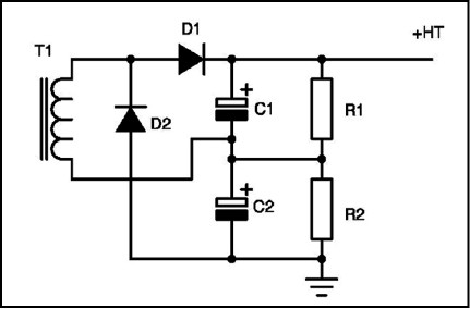
Fig 11.1: Delon voltage doubler circuit.
The high voltage supply for a full-wave bridge will require a higher secondary voltage, and hence more turns on the winding. To account for the 10% regulation factor the use of a multiplier of 1.555 instead of the normal 1.414 factor will be correct. The secondary voltage then needs to be (1250 x 0.707) = 884V AC. Off load it will rise to about 1375V DC for a 10% regulation transformer.
The secondary current required is also determined by the rectifier scheme chosen. For the bridge rectifier (Fig 11.2) feeding a capacitor input smoothing, it will be 1.62 times the required dc output current. If the supply needs to supply 500mA for the valves then the secondary peak current rating needs to be about 800mA.
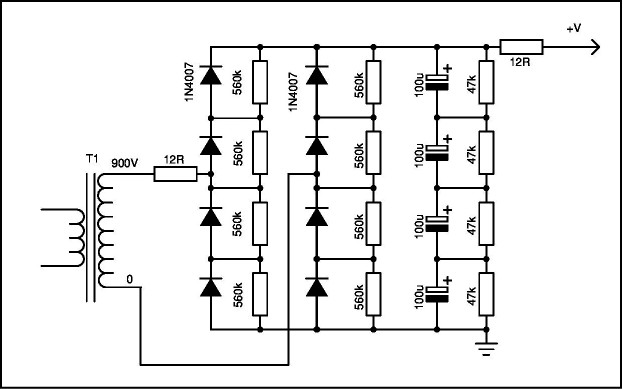
Fig 11.2: Bridge rectifier circuit.
Ripple Voltage
To prevent hum on the transmitted signal the output voltage should be pure DC. The amount that we can tolerate is dependant on the operating mode. Since SSB is an amplitude modulation mode the ripple voltage needs to be low. The percentage of ripple is determined by the amount of smoothing capacitance that is connected across the rectified DC output. The ripple factor is also dependant on the rectifier scheme we choose. For the half wave rectifier we can show that the ripple factor is 1.21 and for the bi-phase and bridge, both of which are full wave rectifiers, the ripple factor drops to 0.438. From this we can see that the full wave rectifier needs a smoothing capacitor value which is lower than that of the half wave rectifier. The half wave rectifier needs a capacitor ~2.5 times larger to equal the full wave types.
Voltage doubler
The popular high voltage supply used by a lot of the commercial amplifier manufacturers is the Delon full-wave rectifier shown in Fig 11.1. Although it also only needs a single secondary winding, and doubles the input voltage, it is in reality two half wave rectifiers working in anti-phase and can be analysed as such. If the mid point in the reservoir capacitor is grounded this can clearly be seen. It is used when we need a split rail supply to supply identical positive and negative voltages at low current. The Delon voltage doubler is not a normal full wave type of supply; it is two entirely separate half-wave rectifiers with the outputs stacked in series. If one diode is removed the other half continues to work unaffected. By moving the ground point to the output of the negative supply (Fig 11.3) it becomes a positive voltage doubler. The two charged capacitors are simply placed in series to double the voltage. The definition of a full wave rectifier is that both halves supply the same polarity DC output, which are summed to provide the total output current. The bi-phase and the bridge are true full wave types, whereas the Delon is not.
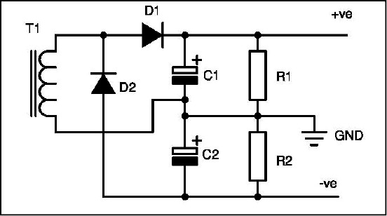
Fig 11.3: Dual split rail supply using half wave rectifiers.
The operation of the Delon voltage doubler can be more easily seen by redrawing Fig 11.1 as in
Fig 11.4, in which the action of the two separate diode-capacitor sections can be analysed. The common point of the secondary winding forces sinusoidal pulses of AC into both the capacitors when the diodes conduct. The raw AC flowing has a peak value of approximately π-times the output DC load current. Hence, the capacitor ripple current is very high.
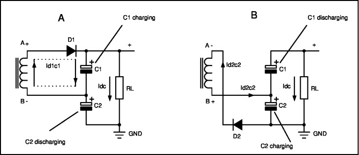
Fig 11.4: Delon voltage doubler operation.
In a half wave rectifier the output voltage is 1.414 times the AC input voltage when the reservoir is a capacitor, the so-called capacitor input filter. The equation for the output current to alternating input current for a half wave capacitor input filter rectifier is:
IDC = 0.28 x IAC
Hence, to achieve 1A DC output current requires (1 / 0.28) input current, which is a factor of 3.57:1. The full wave bridge using the same capacitor input filter requires (1 / 0.62) = 1.612 times the current. The bi-phase rectifier factor is 0.9, so it only needs 1.11 times the DC output current from the secondary winding. The bi-phase option does, however, need two secondary windings, so it is more expensive.
The Delon doubler is named after Jules Delon (1876 – 1941), a French engineer, who patented the design. Originally Delon used a rotary commutator arrangement to form a series of switches – at the time thermionic rectifier valves had not been invented. The two capacitors were individually charged from a DC supply and then connected in series to add the voltages.
For the voltage doubler option, for an output current of 500mA, the secondary current needs to be higher and we have to input 1.78A AC, and when losses are taken into account a value of closer to ~2A is required. This is because the factor is more than doubled compared with a bridge rectifier circuit. This is one of the major failings of the voltage doubler rectifier. It also has a poorer regulation factor than the bridge rectifier. Off load the peak DC voltage is 2.828 times the AC secondary but when the current drawn exceeds about 33% of the maximum the factor falls to closer to 2.25 times. Hence, for the same transformer regulation the output voltage drops considerably more.
In a bi-phase or bridge circuit (Fig 11.5) each diode supplies 50% of the output current, in our example each diode supplies 250mA. In the Delon circuit they both supply the full current. The PIV of the diodes used in a bi-phase rectifier is the same as a half wave rectifier being 2.828 times the output voltage. The PIV of the Delon rectifier diodes is also 2.828 times the output voltage.
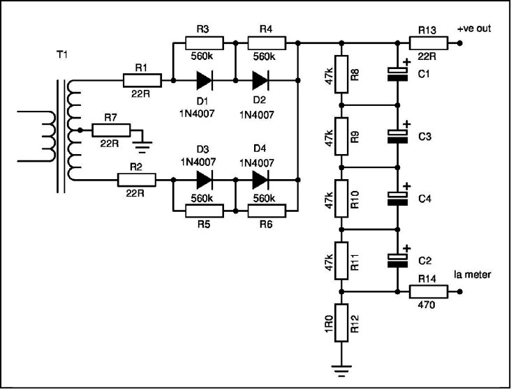
Fig 11.5: Bi-phase rectifier circuit.
In his textbook Electronics and Radio Engineering, Terman makes the following comments about the voltage multiplier circuits: “In general, it can be stated that the full extent of the voltage-multiplying action is present only for very small load currents, and that, as the load current is increased to a moderate value, the output voltage will drop off rapidly. That is, the voltage regulation in these systems is poor.”
A good example of a typical voltage doubler circuit is in the Heathkit SB-230 amplifier. This supply uses a string of seven 1N2071 diodes in each half of the voltage doubler (without any voltage sharing resistors!) The stated voltages for the supply are 2500V when the idle current of 25mA is being drawn and 1900V when the full anode current of 500mA is drawn – it falls by 600V from idle to full load current. This is a regulation factor of 24%. If this was a 13.8V supply then the output voltage would fall to 10.5V on load, which would be regarded as atrocious!
The rectifier diodes are 600V PIV at an RMS current of 750mA, hence they are slightly inferior to the 1N4007 types. The total PIV in each diode string is 4.2kV.
The Heathkit SB-230 high voltage supply, but modified to use 1N5408 in place of the original 1N2071 diodes, is shown in Fig 11.6.
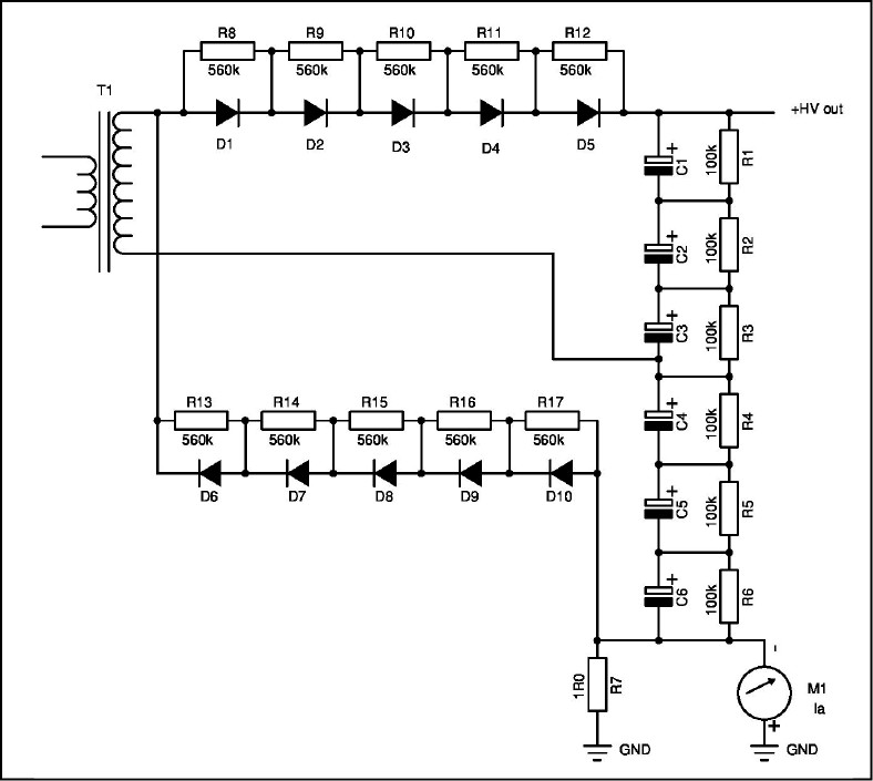
Fig 11.6: Heathkit SB-230 high voltage supply modified to use 1N5408 diodes.
Bridge rectifier
The best choice for high voltage supplies is the bridge rectifier. In this circuit two diodes are connected in series for each pulse of charging current. Although the forward voltage is twice the bi-phase rectifier, the small voltage drop is not significant when a high voltage supply is used. As there are two diodes in series the PIV of each diode can be half that of a bi-phase rectifier, allowing less expensive diodes to be used. The PIV required is two times the DC output voltage. For high voltage operation often several diodes need to be connected in series to attain the required peak inverse voltage (PIV).
The operation of the bridge can be ascertained by redrawing the rectifier to omit the diodes that are not in use for one half cycle. Fig 11.7 shows the two different half cycles and the flow of charging current. The secondary DC return current reverses on alternative half cycles so there is no net magnetising flux in the core.
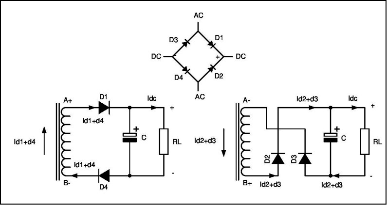
Fig 11.7: Bridge rectifier operating method.
On one half cycle the secondary winding end marked A is positive and B is negative. Diodes D1 and D4 are forward biased and the other two diodes are reverse biased, so they are not part of the circuit for that half cycle. Current flows from A through D1 and then through the reservoir capacitor C and the load RL. The return current flows through D4 back to the other end of the secondary winding. On the opposite half cycle D1 and D4 are reverse biased and only D2 and D3 are active.
Smoothing capacitors
The smoothing capacitor choice is also critical for both types. The capacitor voltage rating must take into consideration not only the off load voltage but also any variation in the mains voltage. In most countries the AC mains has a tolerance of about ±6%. For the 240V mains supply it can vary between 225V and 255V and still be within the legislated limits. This means that the capacitor minimum voltage has to cater for an extra 6% over and above the nominal off load voltage due to the transformer regulation rating. For a 1250V nominal anode supply it can rise to 1460V. If the capacitor is not able to withstand this added voltage it will fail.
As high voltage electrolytic capacitors are normally only available with voltage ratings of up to ~450V we need to connect several in series to attain the required voltage. If four 450V electrolytic capacitors are used the nominal voltage is 1800V and this should cater for most requirements. 450V electrolytic capacitors normally can withstand 525V for brief periods, typically 20 to 100 cycles of the mains, to cater for spikes and surges.
The ripple current rating of the capacitors is also a function of the rectifier type. For the bridge rectifier the ripple current is the same as the transformer secondary current. So a ripple current of 800mA is the minimum required. Most of the larger can size 450V electrolytic capacitors will handle ~1A of ripple current at 100Hz. For the voltage doubler rectifier the ripple current rating is higher, instead of being the secondary current rating it has an additional factor added of ~1.33. Hence, the minimum ripple current rating required is ~2.5A. This explains why a lot of the commercial amplifiers using the voltage doubler rectifier have problems with the smoothing capacitors failing. The lower cost, small can type, electrolytic capacitors do not have the ripple current rating needed and they overheat and explode. The ripple voltage that is required determines the value of the smoothing capacitor.
The standard formula is:
Iavg
C = Farads
8 x fr x Vr
Where:
Iavg is the ripple current flowing in the capacitor
fr is the ripple frequency (normally 2-times the mains frequency)
Vr is the allowable ripple voltage peak-peak value
For a 50Hz mains supply using a bridge rectifier supplying 500mA DC (Iavg of 800mA) with a maximum peak-peak ripple voltage of 50V, the minimum value of capacitor required is 20µF and any capacitor larger than this will provide a lower ripple voltage than 50V.
For this anode supply we would need 4 x 450V electrolytic capacitors connected in series which are (4 x 20µF) = 80µF minimum in value. The closest standard capacitor is 100µF and this would be suitable. This gives a total capacitance of 25µF at 1800V maximum working voltage.
Capacitor ripple current rating
The equivalent series resistance (ESR) and the safe working temperature primarily determine the ripple current rating of an electrolytic capacitor. Today electrolytic capacitors can work up to +105ºC case temperature, but are more expensive than the +85ºC variety. The higher the ripple current the larger the can size needs to be, as the ability to dissipate heat is a function of the can surface area. Small can electrolytic capacitors have higher ESR and have low ripple current ratings.
The voltage doubler option places an extra factor on the ripple current rating of the smoothing capacitors. In a doubler circuit the ripple current is the secondary current times a factor of about 1.33, so the capacitor needs to have a ripple current rating of 1.78 x 1.33 = 2.4A minimum. Many high voltage electrolytic capacitors of 100µF at 450V type cannot handle this sort of current at 100Hz ripple frequency. Typically the upper limit is about 1.25A for a 100µF electrolytic at 450V in the largest can size. Hence, the only safe option is to double up on the capacitors and fit two in parallel. This means that the smoothing capacitor is bulkier and more expensive. It also means we end up with a higher total capacitor value, which is good for ripple suppression but bad for the peak diode charging current. The next standard capacitor is a 220µF, but the ripple current rating is generally not as high as you would assume. It typically is 1.75A for a 450V rating capacitor. So the best option is to parallel two 100µF capacitors rather than using a 220µF.
This example illustrates an important point. Very often the minimum capacitor value required for the ripple suppression has to be modified to cater for the higher ripple current. In many cases it is the ESR, and hence the ripple current, the capacitor can safely handle that determines the minimum capacitor value.
However, as with the transformer, we can use a bit of intelligent abuse. The peak ripple current only occurs for a very short period at the crest of the current peak. The average current is approximately 62% of the peak current, so a slightly lower ripple current may be acceptable if the anode current is not driven to its maximum. If you are in the habit of using a lot of speech compression the rating needs to be much higher, but without excessive compression the peak current is lower.
Typical ripple current rating
There are so many manufacturers of electrolytic capacitors that it is sometimes difficult to assess what is available. As an example I have compiled Tables 11.1 – 11.4 which show what is available from four manufacturers – Nichicon, Hitano, Rubycon and Epcos-TDK – who make a vast selection of capacitors. I have selected a 100µF / 450V radial can type suitable for printed circuit board mounting. The ripple current is quoted at 120Hz at the maximum can temperature.
The Epcos-TDK range are notably superior and are also available in up to 600V rating for some of their types. The data for the ripple is for 100Hz. These types would better suit a voltage doubler circuit.
Type | Can Size DxH mm | Temp. ºC | Ripple Current mA |
LGN | 20 x 35 | 105 | 690 |
LGU | 20 x 45 | 105 | 690 |
LGW | 20 x 30 | 105 | 1040 |
PW | 25 x 50 | 105 | 350 |
Table 11.1: Nichicon 100µF / 450V electrolytic capacitors at 120Hz ripple frequency.
Type | Can Size DxH mm | Temp. ºC | Ripple Current mA |
EFL | 18 x 45 | 105 | 850 |
EHL | 22 x 40 | 105 | 700 |
EHP | 22 x 40 | 105 | 820 |
EHS | 22 x 35 | 105 | 640 |
EHU | 22 x 35 | 105 | 690 |
ELP | 22 x 35 | 85 | 1030 |
ELU | 22 x 35 | 85 | 930 |
Table 11.2: Hitano 100µF / 450V electrolytic capacitors at 120Hz ripple frequency.
Type | Can Size DxH mm | Temp. ºC | Ripple Current mA |
MXG | 20 x 35 | 105 | 910 |
MXH | 22 x 25 | 105 | 850 |
PK | 18 x 40 | 85 | 280 |
PX | 18 x 40 | 85 | 200 |
ULW | 16 x 45 | 85 | 800 |
USC | 20 x 35 | 85 | 880 |
USG | 20 x 30 | 85 | 930 |
VXR | 22 x 50 | 105 | 640 |
Table 11.3: Rubycon 100µF / 450V electrolytic capacitors at 120Hz ripple frequency.
Series | Size |
| Ripple (A) | |
| DxH mm | +60ºC | +85ºC | +105ºC |
B43541 | 25 x 30 | 1.74 | 0.98 | — |
B44544 | 25 x 30 | 2.08 | 1.60 | 0.89 |
B43547 | 25 x 30 | 2.12 | 1.56 | 0.84 |
B43624 | 25 x 30 | 1.58 | 0.90 | — |
B43642 | 22 x 30 | 1.78 | 1.33 | 0.69 |
B43545 | 25 x 30 | 2.06 | 1.52 | 0.82 |
Table 11.4: Epcos-TDK 100µF / 450V electrolytic capacitors at 100Hz ripple frequency.
Electrolytic capacitor technology
Modern electrolytic capacitors have improved dramatically from the earlier types. If one compares what was the norm about 40 years ago with those of today the reduction in size is quite marked. Traditionally a 100µF capacitor of 450V rating occupied a can of 38mm diameter (1.5in) with a height of 75mm (3in) and had a ripple current rating of about 400mA at 85ºC. Today the same value capacitor can be as small as 22mm diameter and only 30mm in height. This often creates a problem when ‘re-capping’ an older amplifier as the new types are too small to fit into the clamps or the printed circuit board. Modern electrolytic capacitors are used extensively in off-line switch-mode power supplies and they have to handle not only the mains ripple frequency but also the high frequency switching currents. These currents sum algebraically to give a much higher peak current.
Today it is quite common to find that the small can size capacitors can handle much higher ripple current than the older types. As an example, a 100µF / 450V can of 38mm would typically handle at the most about 1A of ripple current. The modern capacitor to handle this current can be as small as 16mm in diameter and is rated at 105ºC. With the widespread use of energy saving lamps, which use an off-line switch-mode technology, the sizes are getting smaller.
Capacitor Leakage Current
All capacitors have a small internal leakage current. At low voltage this is not normally a problem. However, in high voltage aluminium electrolytic capacitors the leakage current is largely dependant on the applied voltage and case temperature – the higher the voltage or temperature the greater the leakage current rises. The leakage current rises much faster near the maximum rated voltage and assumes almost an exponential shape in the current versus voltage curve. Although the leakage current is generally small it is still significant. Most capacitor manufacturers publish data on this effect. Generally, the leakage current is defined at maximum working voltage and maximum case temperature. The value given is considered to be the worst case under normal operation. A typical way of stating the leakage current is:
I = 3 V x C
Where:
I is the leakage current in µA
V is the marked maximum working voltage
C is the nominal value in µF
For a 100µF capacitor rated at 450V the maximum leakage current is 636µA (0.64mA).
Sharing resistors
To equalise the voltage across a bank of series connected capacitors a simple method is to form a potential divider chain of resistors. To ensure an adequate bleed current through the sharing resistors it is prudent to make the current at least 10 times the maximum predicted leakage current. For two 100µF / 450V capacitors connected across a 900V DC supply the current therefore needs to be at least 6.4mA. The total resistor value needs to be less than:
R = V / I
= 900 / 6.4mA
~140kΩ
Each resistor needs to be half of the total so they are 70kΩ maximum and the nearest value in the E12 range is 68kΩ. Any resistor values lower than this will suffice and only the power dissipation in the resistor is a concern. For the case of the 68kΩ with 450V across it the power dissipated is:
I = 450 / 68kΩ = 6.6mA
Pdiss = I2 x R or V x I in watts.
Pdiss ~3W, hence a 5W resistor would be suitable.
In commercially manufactured amateur equipment the tendency is to use 470kΩ 1/2W resistors across 450V or 500V electrolytic capacitors, which is far too high a value to be effective. The absolute maximum would be about 100kΩ to have any useful effect. As a good rule of thumb the value of the sharing resistors should not exceed ~10kΩ for every hundred volts of rated voltage.
Capacitor equivalent series resistance
A perfect capacitor would consist of only a reactance. The reactance of a capacitor decreases in value with increasing frequency and we use the normal formula to determine the reactance value. In a pure reactance the current and voltage of an AC applied signal are 90º out of phase and cannot dissipate any power in the reactance. However, smoothing capacitors are not ideal items and some additional series resistance exists. This is known as the equivalent series resistance (ESR) and being a resistance it does dissipate power as heat when a current flows. The ESR value of a typical high voltage electrolytic capacitor is generally not of great concern as long as the ripple current is not too high.
If the various manufacturers’ data sheets are examined, often the ESR value is not quoted for the types intended to be used with low ripple frequencies. For switch-mode power supply capacitors ESR is the major loss factor and ESR generally decreases with rising frequency. At 120Hz the ESR is considerably larger than at 100kHz, and this is inferred by the derating factor for the ripple current. Very often, for the types designed for switch-mode supplies, the ESR is given as the impedance value in ohms.
If the reactance of a 100µF / 450V electrolytic is calculated, at 100Hz it has a reactance of ~16Ω. The maximum ripple current is typically 1A. Hence, the maximum RMS ripple voltage is limited to 16V, which in peak-peak values is ~45V. However, if the ESR is 12Ω the effective impedance is:
Z = (X2) + (R2) = 20Ω
Hence, the ripple voltage can be increased to 20V RMS (~56V p-p) before the 1A limit is exceeded. At this ripple voltage the 1A flowing in the 12Ω of ESR dissipates 12W which will heat up the capacitor.
Capacitor Working Voltage
It is prudent not to utilise the total working voltage range so as to cater for short term mains disturbances (transients etc) which raise the input voltage. Consequently, it is considered good design practice to limit the applied voltage to be not greater than ~85% of the rated working voltage. Another factor is the mains regulation. In many countries the AC mains has a ±6% tolerance and for the UK mains of nominally 240V the lower and upper limits are 225V to 255V.
In the above example three electrolytic capacitors connected in series would be a better option. As the off load voltage is not likely to exceed about 115% of the full load voltage, the choice of 3 x 450V working capacitors would be appropriate. When operated at 85% of the rating this gives 3 x 385V = 1155V nominal rating. The 115% voltage would be 1035V. The maximum capacitor voltage rating is 3 x 450 = 1350V. This leaves a safety margin of ~300V to cater for mains borne transients and mains tolerance variations.
For this smoothing capacitor bank the sharing resistors could be 3 x 33kΩ = 99kΩ. The bleed current through the resistors is 900V / 99kΩ = 9mA, which is higher than the required 6.4mA. The total dissipation in the resistors is ~8.2W and since this is shared by the three resistors it is 2.73W per resistor. A 5W type would be appropriate for reliability.
Total transformer power rating
In order to assess what transformer is required, we need to add up the various supply details and then calculate the total VA rating. Each 811 valve requires 6.3V at 4A for the filament heater. The filament supply would be 6.3V at 12A = 75.6VA.
The anode supply requires ~900V at 800mA for a bridge rectifier (720VA) and the doubler option requires ~443V at ~2A (886VA).
Any additional supplies, such as a –100V bias supply, will be low power windings and 50mA AC RMS would be adequate at a secondary voltage of 70V and a rating of ~10VA would cover most applications. For relays, an additional 20VA would be suitable.
So our total VA rating at 100% duty cycle is:
Bridge option = (75.6 + 720 + 30) = 825VA
Doubler option = (75.6 + 886 + 30 = 992VA
This could be intelligently de-rated by about 40% to give a figure of 500VA for the bridge and 600VA for the doubler.
The major problem with the voltage doubler rectifier option is that the peak flux in the transformer core is considerably higher than for the bridge option. This normally means that the frame size needs to be bigger to prevent saturation. This makes the transformer larger and more expensive than the equivalent bridge rectifier option.
Rectifier diodes
The choice of suitable high voltage rectifier diodes is also important. The PIV value needs to have some safety margin to handle any transients and spikes on the input supply. As there are four diodes in the bridge, and diodes are arranged in series pairs, the total PIV required must be at least two times the output voltage. If we estimate that the off load voltage worst case is about 1600V, we need a minimum PIV of twice this value. Two 1kV diodes in series in each leg will be adequate. If 1kV diodes are selected this gives a PIV of 4kV, which is well above the required value.
For the bridge rectifier, a diode with an average current rating of at least 1.5 times each secondary current of 400mA means that a 0.6A rating is the lowest suitable. The voltage doubler rectifier diode current would be a much higher value. The secondary current is approximately 1.8A average and this is courting disaster with such a slim margin. It hence needs diodes with at least 3A average rating.
The doubler option will also need diodes in series in each section as the minimum required PIV is 2.828 x Vout. Assuming the off load worst-case anode voltage is also 1600V, the PIV required is at least 4.5kV. Hence, the absolute minimum number, if using 1N5408 diodes, would be five – and six diodes would be a safer option. This requires 12 x 1N5408 diodes. The bridge can use 8 x 1N4007 diodes.
When diodes are connected in series a voltage-sharing resistor is required across each diode. A 330kΩ to 560kΩ 1/2 watt resistor would be suitable. Damping capacitors are not required and they can cause unwanted avalanche effects, so they are undesirable with modern high-voltage rectifier diodes. They were used for earlier rectifier diodes but were fitted to suppress RFI from the switching. Modern diodes switch at least five times faster and generate very little RFI.
Choice of Rectifier Type – Which Would You Choose?
As you may have surmised by now, I am not a big fan of the voltage doubler circuit. It persists for all the wrong reasons! The claimed advantage is that it needs fewer turns on the secondary winding. That may be so, but it also needs 2.66 times the copper area to equal the bridge rectifier. Copper today is an expensive commodity. The lower labour cost of winding less turns is more than exceeded by the extra cost of the copper required and also the larger transformer frame size to carry the higher magnetic flux. When it boils down, the cost saving of fewer turns on the secondary is totally negated by the other costs. However, it’s your money so you can decide which type you prefer.
If I had a choice I would list the options in this order:
1 Bi-phase – choke input filter
2 Bi-phase – capacitor input filter
3 Bridge – choke input filter
4 Bridge – capacitor input filter
5 Delon doubler (but only if I was forced to!)
Centre tapped secondary
Here is a tip about the bridge rectifier. If a centre-tapped secondary is used we have the ability to improve the voltage sharing. Although a bridge rectifier doesn’t require a centre tapped secondary, I always use one. By connecting a wire from the centre tap to half-way down the capacitor bank (Fig 11.8) it forces that point to be exactly 50% of the output voltage. This of course means you have to use an even number of capacitors in series, but that isn’t normally a problem. I would rather add an extra capacitor and know I have ample voltage rating in hand than worry about the capacitors being run too close to their limit. The addition of a centre tap when winding a transformer is a very small increase in the cost.
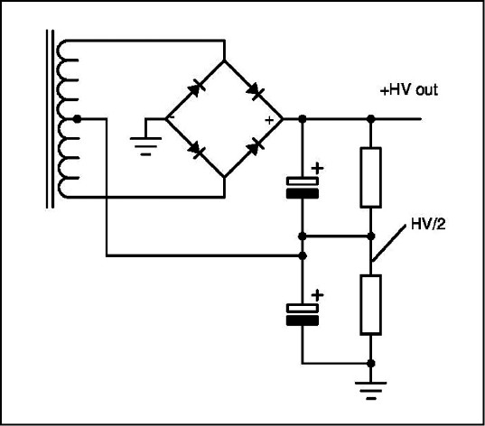
Fig 11.8: Centre tapped secondary bridge rectifier circuit.
Another benefit of a centre-tapped secondary is that it provides the option to supply another part of the circuit with a lower voltage at a current of up to about 25% of the main output current. This may be used to supply a screen voltage stabiliser for a tetrode valve, saving an extra secondary winding, rectifiers and smoothing capacitors.
Tetrode amplifier supply
The tetrode valve, including the beam tetrode family, requires an additional positive voltage supply to feed the screen grid. In most cases this needs to be a very stable voltage that does not vary with anode current or the current that the screen grid draws. It is especially critical for some valve types such as the 4CX250 / 350, where the screen grid not only demands current from the supply but also supplies current back into the supply. This second current is known as negative screen current and is a potential cause of damage to the valve.
The shunt regulator is the best method to counter the need for both a positive and negative screen current, whilst also limiting the positive screen current to a safe value. Most tetrode valves will benefit from a proper shunt regulator and provide better linearity with a stiff and stable screen grid supply. If the screen voltage wobbles around due to anode current flow higher levels of IMD will be generated.
A simple shunt screen regulator suitable for most tetrode valves and using a high voltage IRF-840 MOSFET as a variable resistance element to hold the output voltage constant is shown in Fig 11.9. This stabiliser can hold the screen grid voltage within 20mV of the required target voltage.
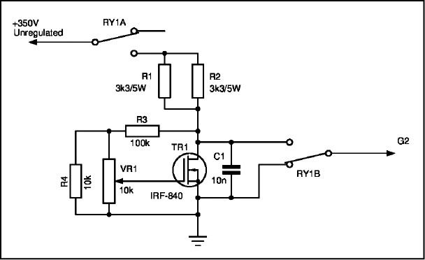
Fig 11.9: Screen grid shunt stabiliser.
The output voltage is determined by the value of R3; increasing its value raises the output voltage. VR1 allows adjustment of the output voltage over a wide range. The maximum screen grid positive current is determined by the value of the series dropper resistors R1 / R2. The unregulated supply needs to be high enough to cater for the valve screen grid voltage required and an overhead of about 100V normally suffices. The values shown suit a valve such as the QQV06-40 or 4CX250 for a +250V screen grid supply. The relays turn off the stabiliser on receive and ground the screen grid pin. Hence, no power is wasted in the regulator when it is not being used. TR1 must be mounted on a heat sink with an isolating washer and bush to prevent shorting the drain tab to ground. Do not increase the value of C1 by more than 25% as this component determines the loop response time to changes in the output voltage. If large additional smoothing capacitors are added the regulator will not be able to follow the changes fast enough.
Grid bias stabiliser
Where a very stable grid bias supply is required another simple stabiliser can be used. The stabiliser shown in Fig 11.10 uses a common high voltage NPN transistor (BU406) to obtain a very stiff and stable negative supply voltage.
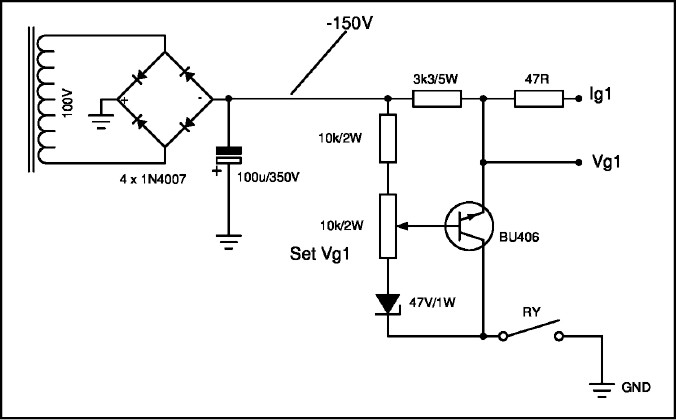
Fig 11.10: Grid bias stabiliser.
The transistor is operated as an emitter follower with low output impedance. The values shown suit an output voltage of about –45V to –75V. Cut-off biasing during receive is performed by the relay contact that lifts the bottom of the potential divider up from ground. In this condition the output rises to the unregulated input supply rail of about –150V. The transistor needs mounting on a heat sink with insulating hardware to prevent shorting to ground. Grid current monitoring is by the 47Ω resistor in series with the output. This value can be changed to suit the moving coil meter used.
Microwave oven high voltage transformers
In the quest to save money some amateurs have experimented with microwave oven transformers. On paper they look attractive, they are capable of fairly high power output and have a secondary winding of about 2.2kV. However, they are not suitable for an amplifier. The reason is because they are designed in a particular way.
The magnetron in a microwave oven operates with a half wave rectified anode voltage of about 5 to 6kV. The secondary winding is applied to a special voltage doubler circuit, normally using a series capacitor of about 1µF and shunt diode. The output voltage is a negative polarity. The high voltage negative DC supply is applied to the cathode of the two-electrode magnetron valve. It behaves like a half wave rectifier valve. The anode is bolted to the waveguide and sits at ground potential.
If it were not current limited the magnetron would try to draw a very high current. Consequently the transformer is constructed to have a flux limited core by fitting magnetic shunts in the magnetic circuit. This causes the transformer to behave like a constant current source and limits the magnetron current to a safe level, typically about 200 to 300mA. The transformer laminations often have an additional air-gap between the limbs to assist the magnetic shunts and the whole thing is arc welded together. You can dismantle them, but it is a lot of effort and the danger exists of damaging the windings. The filament winding is normally a 3V / 30A secondary to power the cathode filament. This is connected internally to the negative output so it is sitting at about 5kV above ground. Although it is possible to modify them it is not worth the trouble and expense.
An economy high voltage supply example
Finding a suitable transformer sometimes can be fraught with difficulty. It is sometimes possible to utilise transformers that at first sight aren’t what we really want. Amongst my collection of mains transformers I came across two identical transformers that were in good condition, but had 115V primary windings. Each transformer has a high voltage secondary winding of 700V centre tapped, so in British parlance they are 350-0-350 types. The secondary was rated at 200mA and there were also two heater windings of 6.3V. One was centre tapped at 3.15-0-3.15 at 8A and the other was 6.3V at 3A. As I required a ~1kV supply this proved to be workable.
The secondary windings were connected in series to form a bi-phase rectifier feeding a bank of electrolytic capacitors. In the bi-phase rectifier the centre tap is the ground terminal, so it wasn’t possible to form a half-rail supply (as with the bridge) to force the capacitor bank to the half voltage point. But by utilising the secondary centre taps a second bi-phase rectifier was arranged to give this feature.
The two transformer primary windings can be connected in series to operate from 230V or in parallel for 115V input. When connecting in series or parallel the phasing of the primary windings is important. If the phasing is incorrect the rectifier acts as two paralleled half wave rectifiers. By swapping the polarity of one transformer primary the correct phasing is provided. Each diode needs a sharing resistor across it to equalise the breakdown voltage. The electrolytic capacitors selected were 100µF/400V Hitano ELP series which are rated at ~1A ripple current at +85ºC. These are low cost and have a 22mm diameter case, so they occupy little space. The schematic is shown in Fig 11.11.
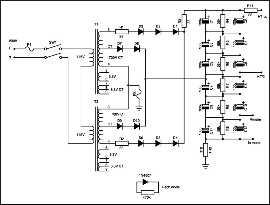
Fig 11.11: An economy power supply using 115V transformers.


