Chapter 8 -
Reverse Engineering Xbox Security
In this chapter, I will describe how I defeated the initial production version of the Xbox security system that was first encountered in Chapter 6. The security system was discovered after analyzing the FLASH ROM and realizing that the true hardware initialization and boot image decryption sequence was somehow hidden outside of the FLASH ROM. The Chapter 7 introduced some basic cryptography concepts that will be useful understanding the contents of this chapter.
Extracting Secrets from Hardware
The hidden boot code in the Xbox, as concluded in Chapter 6, can be recovered by eavesdropping on one of the following buses: (1) the FSB, (2) the main memory bus, or (3) the Northbridge-Southbridge connection.
The format of the Front Side Bus (FSB) of the Pentium processor used in the Xbox is documented in the Pentium III processor datasheets, available at Intel’s Developer Website. The FSB is a bidirectional 64-bit data bus with about fifty address and control signals, all running at 133 MHz. The bus uses a signaling convention known as AGTL+. Eavesdropping on this bus is an expensive and difficult proposition because of the high signal count and challenging physical form factor. Viable approaches include: (a) socketing the processor with a special emulator break-out socket that costs many thousands of dollars, or (b) reverse engineering the meaning of each FSB trace on the Xbox motherboard, and tack soldering a short probe wire onto each of the almost one hundred signals. In addition, a logic analyzer that supports AGTL+ signaling is required. The combination of all these factors made me look elsewhere for a starting point for eavesdropping.
Our next eavesdropping candidate, the main memory bus, is a 128-bit data bus plus address and control signals running at 200 MHz with double data rate (DDR) clocking. The memory bus uses a signaling convention known as SSTL-2. (The details of this bus can be inferred by reading the datasheet for the Samsung K4D263238M memory part, available at the Samsung Electronics website.) Despite its higher speeds, eavesdropping the main memory bus is probably easier than eavesdropping the processor FSB, because of the empty (spare) memory footprints designed into the Xbox motherboard.
A relatively inexpensive, standard 100-pin TQFP adapter (Thin Quad Flat Pack, a rectangular chip package with 100 gull-wing shaped pins) could be soldered onto the empty memory footprints. These adapters would provide convenient probe points for connecting a logic analyzer. The problem with this approach is that you can only capture data that is written to main memory. Decryption keys are generally read-only data, and read-only data will go straight from the hidden boot ROM into the processor cache without ever being stored into main memory. Once the processor is done with the cache line containing the key, it will be overwritten, so the key should never leave the physical perimeter of the processor.
More About High Speed Information Transmission
Eavesdropping and modifying data on computer buses is a powerful technique that is difficult to counter. In order to understand how to eavesdrop, you will need a little bit of background on how digital information is transmitted inside a computer.
There are two major categories of signaling standards: single-ended and differential. The transmission of digital information over a wire requires a translation into physical quantities such as voltage and current. Classically, signals were defined in terms of voltages measured with respect to a common reference potential called the “ground.” This kind of signaling is known as single-ended or unbalanced signaling. Unfortunately, the idea of a ground reference point only works when signals change slowly with respect to their propagation time. In reality, every change in potential is accompanied by a flow of current. The laws of nature demand that current be conserved, i.e., for every flow of current in one direction, there must be a flow of current in the reverse direction. In single-ended signaling, the reverse current, also known as a return current, must find its way back through the “ground”. At very high speeds, the return paths for current do not necessarily follow the same path as the signal current. This imbalance results in a distorted signal.
Differential signaling combats this problem by using two wires to transmit a signal, with one wire used for the signal current and the other used for an explicit return current path. The differential approach allows the signal and return paths to be laid out so that they track each other, ensuring that the flow of current is balanced. The result is a more robust signal transmission system at the cost of twice the number of wires.
A specific standard for interpreting voltages as logic values is called a signaling convention. The venerable TTL and 3.3V CMOS signaling conventions were invented in an era when transistors performed so poorly that large signal excursions were necessary. Lately, a host of new and even old signaling conventions have been gaining popularity, such as SSTL (series stub terminated logic), GTL (gunning transceiver logic), LVDS (low voltage differential signaling), and PECL (pseudo emitter coupled logic). These high-speed signaling conventions account for the fact that electric waves travel slowly with respect to the rate of data transmission. They also account for the fact that electric waves carry energy that must be dissipated upon the termination of its journey, otherwise the energy will reflect and cause interference with incoming waves.
In high-speed applications, wires are often called “transmission lines” in order to emphasize the fact that these waves travel slowly in comparison to the signal transition time (the time required for a signal to transition between a “1” and a “0” state). (Note that the speed comparison is made relative to transition time of the signal, and not its gross signaling frequency.) A common mistake is to think that transmission line effects can be ignored because the clock frequency of the signal is slow. Even if there is only one transition every year, problems can still arise if the duration of that transition takes only a picosecond (one trillionth of a second).
The good news for novices is that the latest FPGAs from vendors such as Xilinx come with built-in support for almost every widely deployed signaling standard. The other piece of good news is that signaling standards are becoming increasingly well documented. The Xilinx FPGA data sheets, for example, illustrate the expected position and value of the termination resistors for every supported signaling standard. By following the recommended practices in the datasheet and application notes, you can use the FPGA to eavesdrop on a wide range of signals. Just remember to keep your eavesdropping taps as short as possible and you shouldn’t go wrong.
The third potential eavesdropping candidate, the Northbridge to Southbridge connection, is a pair of unidirectional, 8-bit wide differential busses, each with just one control signal and one clock signal. The bus uses the HyperTransport signaling convention and runs at 200 MHz with DDR clocking. The signaling convention of the bus was deduced from the publicly available information at nVidia’s website about the nForce, a chipset closely related to the Xbox’s chipset. A few measurements with an oscilloscope, cross-checked against the open HyperTransport specifications available at the HyperTransport consortium’s website, were used to verify the assumption that the HyperTransport signalling convention is indeed being used.
The HyperTransport bus is implemented on the Xbox motherboard with all the signals parallel and evenly spaced, a decision likely driven by the high operating speed of the bus. This makes the bus an ideal target for eavesdropping, except for the fact that it runs at such a high data rate. Eavesdropping a bus that runs at this speed requires special attention to the stub length of the eavesdropping traces (in order to preserve the integrity of the signals) and it also requires a rather expensive logic analyzer or a custom analyzer circuit.
Ultimately, the Northbridge-Southbridge connection was chosen as the first bus to eavesdrop because it has by far the fewest wires, and therefore requires the least amount of soldering. The Northbrige-Southbridge connection has only ten unique signals, whereas both the FSB and the main memory have about one hundred signals each. Soldering a large number of connections not only consumes a large amount of time, but also greatly increases the risk of hardware failures due to solder bridges or damaged traces. Thus, minimizing the number of solder connections minimizes the risk of collateral damage to the motherboard.
Eavesdropping a High Speed Bus
I had committed to the HyperTransport eavesdropping approach in late January 2002. The significant technical issues with this approach were:
• Tapping the high-speed differential bus without disrupting signal integrity
• Finding or building a logging tool that could keep up with the 400 MB/s data rates on the HyperTransport bus
• Determining the polarity and bit ordering of the differential HyperTransport bus traces on the motherboard
Tapping the Bus on a Budget
The first two issues are intimately linked. High-speed bus analysis and logging tools typically have proprietary interfaces that would require a custom adapter to the Xbox motherboard. The last issue, determining bit polarity and ordering, just requires a lot of post-processing and data massaging after the data logger is attached and functioning.
HyperTransport is an open standard that has gained industry acceptance, meaning that off-the-shelf protocol analyzers and logging tools are available for the bus. One such example is the HyperTransport protocol analyzer by FuturePlus. Unfortunately, this protocol analyzer was priced in excess of $25,000 at the time the work was being done. In addition, the protocol analyzer requires the target board to be specially designed to accommodate the protocol analyzer’s bus interface pod.
Instead of buying a protocol analyzer and investing the time and effort to adapt it for use with the Xbox, I built my own simplified one. This task is feasible because the HyperTransport protocol is quite simple. The Xbox implementation of HyperTransport uses two 8-bit unidirectional buses, one for transmit and one for receive. Each bus has a clock and a strobe line associated with it. The signaling standard requires valid data to be presented on each edge of the clock. The beginning of a new packet is indicated by the data lines leaving their idle state. The strobe line differentiates between command and data packets. All of the sideband signals typical of other busses, such as the address, read/write control, chip select, and interrupt lines, are handled in HyperTransport using in-band command packets. Hence, just ten differential signals (twenty wires) are all you need for eavesdropping the bus — great news for hackers.
The HyperTransport protocol is simple enough, but what about finding something that can both physically interface to the Xbox bus and keep up with the 400 MB/s speeds? The ideal tool for building this HyperTransport bus tap would be an FPGA. However, at the time, no FPGA was available that could keep up with the high data rates and more importantly, no FPGA was available that was certified by the vendor for use with HyperTransport. Theoretically, a Xilinx Virtex-II FPGA would work for this application, but the product had just been launched and the devices were extremely pricey and hard to get (today, you can purchase a low-end Virtex-II FPGA for well under a hundred dollars). The best FPGA that I had on hand at the time was a Xilinx Virtex-E FPGA that I had previously designed into a prototype supercomputer network router as part of my thesis. The network router board used CTT (Center Tap Terminated) signaling for its network interfaces, and also had an Intel StrongArm processor on board for configuration, control, and debugging purposes.
The challenge therefore boiled down to figuring out how to interface HyperTransport signals to CTT signals, and how to coax 400 MB/s performance out of an FPGA that wasn’t intended to run at those speeds.
The HyperTransport signaling convention, it turns out, is a close relative of the more common LVDS (low voltage differential signaling) convention, specified in the TIA/EIA-644 standard. HyperTransport drivers create a signal with a differential swing of 600 mV typically, centered around a common mode voltage of 600 mV. LVDS receivers, on the other hand, can make sense out of data that has a differential swing of greater than 100 mV and a common mode voltage anywhere between 50 mV and 2.35 V. So LVDS receivers are directly compatible with HyperTransport drivers! (Although the Virtex-E supports a direct interface to LVDS signals, I could not take advantage of this because the Virtex-E parts I had were already designed into a system that is hard-wired for CTT signals.) If you are designing your own tap board, the best approach would be to use the native LVDS capabilities of the FPGA instead of the hack described here. In addition, the LVDS receiver must be located very close to the Xbox motherboard in order to not corrupt the target signals. A long cable would dissipate energy out of the wires and introduce noise and reflections that might cause the system to cease functioning.
What About Driving Signals onto HyperTransport?
The eavesdropping application described in this chapter only requires a HyperTransport receiver. Applications such as “man-in-the-middle” attacks require a device that can override HyperTransport signals and insert a false bit or two. Such a device is feasible because HyperTransport, like LVDS, uses current-mode drivers. In other words, the drivers are designed to drive only a measured amount of current into the wire, regardless of the voltage it creates. In a normal situation, this works perfectly well because the impedance of the wire transforms the current into a voltage in accordance with Ohm’s Law. However, currents can sum and cancel each other out. An antagonistic differential driver that applies an overdrive current that cancels out the intended signal can be attached to a HyperTransport line. This kind of overdrive can be accomplished using the flexible, programmable I/O provided in FPGAs such as the Xilinx Virtex-E and Virtex II.
The simplest application of such a bus override device would be one that modifies the destination of the reset vector as it is transmitted to the CPU, enabling you to gain control of the Xbox. The reset vector destination is coded into a single byte that follows the “jump” opcode located at 0xFFFF.FFF0. The reset vector is likely transmitted a deterministic number of clocks from the de-activation of reset, so the timing element for this attack can consist of just a timer that is clocked by the HyperTransport bus clock and synchronized to a reset signal. A “man-in-the-middle” attack like this wil defeat even a cryptographically secure public-key boot block implementation.
The solution to the problem of getting the HyperTransport signals to the FPGA is to use a signal conversion chip. LVDS is a popular standard for LCD panel interfaces and backplanes used in telecomm systems, so numerous inexpensive LVDS-to-CMOS converters are available. Of course, the desired signaling convention is CTT, but a closer look reveals that interfacing CMOS drivers to CTT receivers is actually not a problem. CTT is a current-mode signaling convention that drives +8 mA or -8 mA into a 50 ohm transmission line terminated at 1.5 volts. The receiver is a differential amplifier that compares the reference termination voltage with the transmission line voltage. In the Virtex-E, a CTT receiver amplifier is specified to work as long as the received voltage swings more than 200 mV up or down from the reference voltage. Most CMOS transmitters driving a CTT terminated line will have no problem sourcing or sinking 8 mA of current into a 50 ohm load. Also, CMOS transmitters should have no problem driving a wire terminated into a fixed voltage. Thus, a standard LVDS to CMOS converter chip can be used to take the Xbox motherboard’s HyperTransport signals and feed them into the board I had previously built for my thesis. The chip I chose was the Texas Instruments SN65LVDS386, and you can find data sheets for this chip at Texas Instruments’ website.
Attaching the LVDS-to-CMOS converter chip to the board is made delightfully simple by the clean layout used for the HyperTransport bus on the Xbox motherboard. Figure 8-1 is a picture of what the HyperTransport bus traces look like. Notice how all the wires run in parallel and how they are evenly spaced. Some of the wires, such as the clock (TX CK/TX CX* and RX CK/RX CX*) and the strobe line (TXD8/TXD8* and RXD8/RXD8*), are even labeled for us with polarity markings! This simple layout enables the use of an easy-to-engineer tap board.
The tap board contains just the LVDS-to-CMOS converter chip, some power conditioning circuitry, and a set of traces laid out right up to the edge of the board that are identically spaced to the HyperTransport bus on the Xbox motherboard. For identical spacing and easy alignment and mounting, I measured the dimensions of these traces using a digital caliper tool. Figure 8-2 illustrates the dimensions of the HyperTransport bus traces.
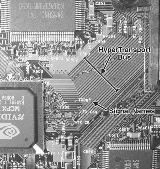
Figure 8-1: HyperTransport bus traces as laid out on an Xbox motherboard.
The measurements were a little tricky to make. My approach was to measure the overall width of the bus and divide the width by the number of traces and spaces to get the average expected spacing and trace width. I then laid out these traces with a PCB CAD program and printed the layout on paper at a 1:1 scale. I compared the printed traces with the board traces and made a few adjustments by hand. (Note that many printers have some small amount of scaling error, so if you are trying this, calibrate yourself by printing out a few long lines of known length and measuring them. Printers can have different scaling errors along the horizontal and vertical axes, so be sure to print lines in both directions.)
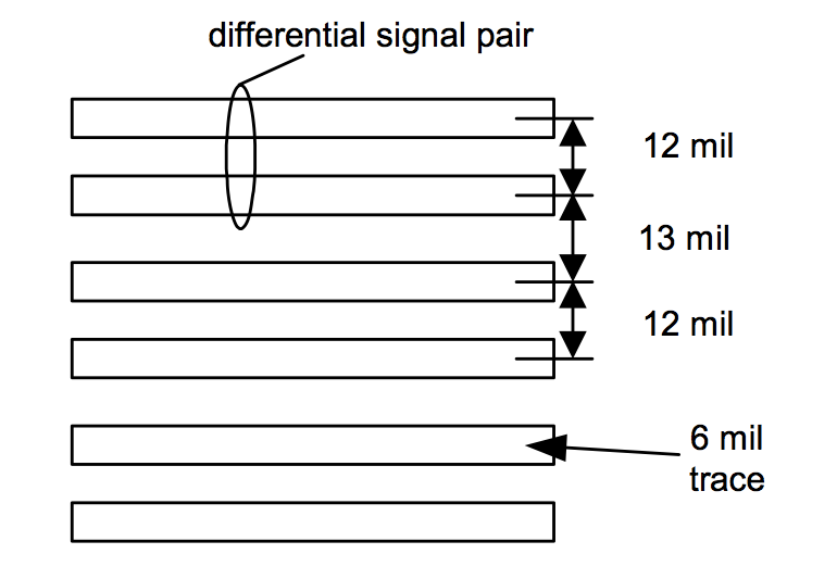
Figure 8-2: Dimensions of the HyperTransport bus traces on the Xbox motherboard. A “mil” is 1/1000th of an inch or 25.4 microns.
Designing your own boards is fairly easy with the right software. You can find out more about how to make your own boards by reading the Appendix C, “Getting Into PCB Layout.”
Once the component selection process was finished, the design and layout of the HyperTransport tap and signal conversion board took just a few more hours. A schematic of the board’s design can be seen in Figure 8-6. The board was then fabricated by an order placed via the Internet. Many board houses offer affordable, quick-turn board fabrication services that take board designs in Gerber file format via an email or ftp upload. In this case, I had two copies of the board built in five days for a price of $33 per board (see Appendix C, “Getting Into PCB Layout,” for more information on how to build your own boards). This price only includes the price of cutting the board into a square piece. However, I needed the side of the board with the HyperTransport tap to have a special shape that facilitates board mounting without interfering with the existing components on the Xbox motherboard. I also needed the mating edge of the board to be beveled such that the board mounts at a slight angle, to simplify the task of soldering the tap board to the motherboard. I used a belt sander to manually sculpt the edge into the shape described in Figure 8-3. When sculpting, the board had to be oriented such that the belt sander’s abrasive belt made contact with the trace side of the board first to prevent the belt sander from tearing the copper traces off of the board. Be careful when using a belt sander to sculpt small boards like the tap board — a belt sander could just as easily sculpt your fingers by accident.
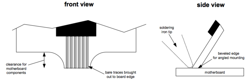 Figure 8-3: Shaping of the HyperTransport tap board edge.
After sculpting the beveled edge, all the parts were soldered onto the board. (See Appendix B, “Soldering Techniques.”)
The finished tap board now had to be attached to the Xbox motherboard. This critical step was perhaps the most difficult one. First, the Xbox motherboard was prepared by using a fine grit sandpaper to strip away the green soldermask, revealing the bright bare copper of the target traces. Then, these traces were fluxed and a thin coat of solder was applied using a hot soldering iron tip.
The procedure I used for attaching the tap board to the motherboard is shown in Figure 8-4. The prepared tap board was tacked onto the motherboard at the approximate location and angle using a thin (30 AWG) wire soldered between a trace on the tap board and the motherboard. The tack wire serves only as a temporary aid for holding the board in place and will be removed, so it does not matter if the wire bridges multiple traces. Once the wire was attached, I carefully adjusted the position of the tap board on the motherboard, heating the wire to release its bond to avoid lifting any of the copper traces. (I used a microscope to aid in determining the optimal alignment.) Once I was satisfied with the position of the board, I applied a strong epoxy to the board joint to hold it all in place. The epoxy should cure and form a rigid, stiff joint. (Note that some epoxies when applied incorrectly cure into a gel; this is not acceptable, as the entire mechanical integrity of the joint must come from the epoxy and not the solder joints.) I used Miller-Stephenson Epoxy formula 907, and it sets with enough strength for me to lift the Xbox by the tap board and not disturb the tap connection.
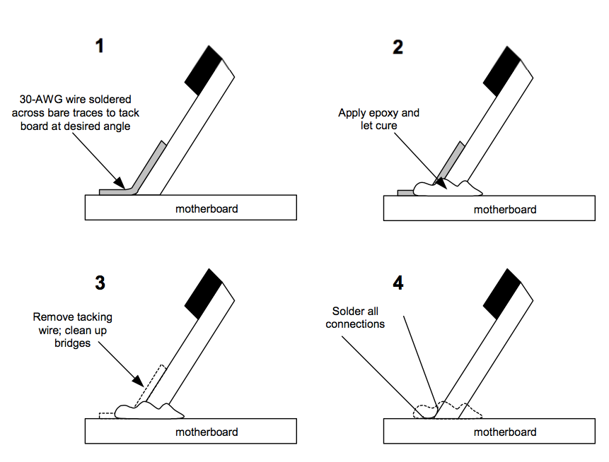
Figure 8-4: Tap board soldering procedure.
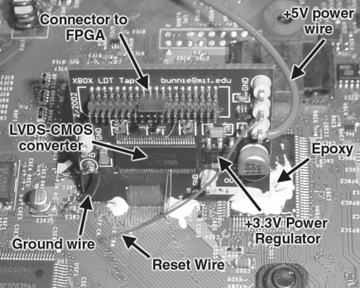
Figure 8-5: HyperTransport tap board mounted on the Xbox motherboard.
Once the epoxy had cured, I removed the temporary tack wire that was used to hold the tap board in place, and cleaned the bare mated traces with a bit of solderwick and flux. The last step of soldering the tap board traces to the bare motherboard traces was now no different from soldering any surface mount component onto a board; most of the standard techniques described in Appendix B applied directly to this situation. Figure 8-5 shows what the finished assembly looks like.
Building the Data Logger
The second challenge of eavesdropping the HyperTransport bus is acquiring or building a logging device that can keep up with the 400 MB/s data rate of the bus. Considering my budget, I decided that my only option was to build a logger, as buying any tools with sufficient performance for this job was well outside of my budget.
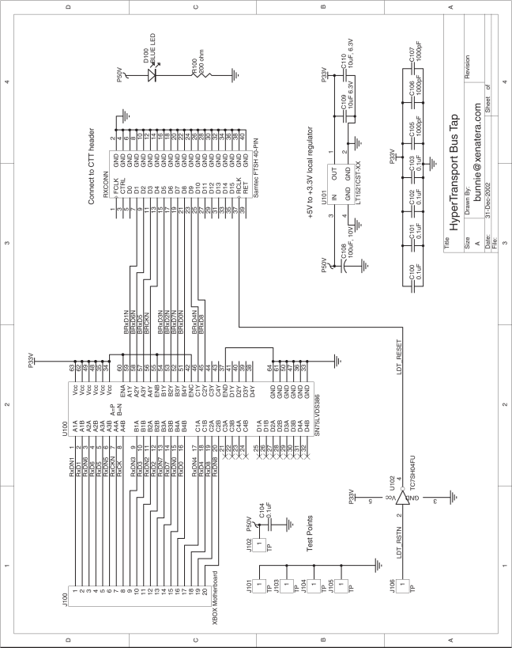
Figure 8-6: Schematic of the HyperTransport tap board.
In building the logging device, I had settled on using a Virtex-E FPGA that was integrated into a board that I had previously built. However, the one problem with using the Virtex-E FPGA is that the performance of the FPGA (as specified in the databook) is insufficient to keep up with the HyperTransport bus. Fortunately, FPGAs overclock well because their manufacturing margin is very conservative, and because FPGA performance is largely limited by signal propagation delays in the configurable wiring fabric. As a result, some key performance-limiting paths can be manually identified and compensated using soft delay lines and selectively inverted clocks. The most performance sensitive blocks can be hand-placed to optimize the delays, while the compiler and automated place-and-route tool handle the non-critical parts of the circuit. Figure 8-7 shows the overall design that was used to capture the data on the HyperTransport bus.
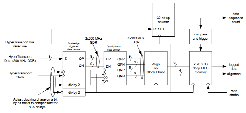
Figure 8-7: Block diagram of the data logger built in the Xilinx Virtex-E FPGA.
The design is fairly simple in concept: take the high speed data off of the HyperTransport bus and clock it into four phases of a quarter speed clock, creating a data stream that is four times slower but four times wider. This confines all hand-placing and tweaking to just the first few input flip flops. Next, realign the data using a set of delays and rotators, and store the data one piece at a time inside a first in, first out (FIFO) memory. The signal that triggers the start of FIFO capture is generated by a timer-comparator that starts counting up from first reset. Long windows of data can be captured by concatenating the results of multiple runs, each with the capture trigger point delayed from the previous. A later optimization applied to the trigger circuit is a “do not store zeros” (DNSZ) function. In the DNSZ mode, data consisting of all 0’s is not stored in the FIFO. This is helpful in culling out all of the idle data on the HyperTransport bus. The resulting data traces are a time-stamped series of 32-bit words.
The most difficult part of the FPGA data logger design was calibrating the delays on the input paths. Delay calibration was accomplished by using an oscilloscope to probe a small window of data on the HyperTransport bus. Wire delays and byte-wide rotations were tweaked until the probed data matched the log data. This process was aided by the fact that during idle times, a common sequence of commands was repeated on the bus every few hundred microseconds, which served as the calibration reference.
Determining the Bus Order and Polarity
The final challenge after logging the data is figuring out the order of the signals on the HyperTransport bus and their polarities. Note that while the two most important signals of the HyperTransport bus on the Xbox motherboard are labeled for us, the remaining eight data lines have ambiguous polarity and bit ordering.
The correct polarity of the eight data signals was determined by observing the idle bus data bit pattern. The HyperTransport bus spends most of its time in an idle state, so this is not difficult. If the idle pattern is supposed to be all 0s, then any bit position that shows up as a 1 has its polarity inverted. This was corrected in hardware by inserting an inversion term in the FPGA on the appropriate wire.
Determining the correct bit ordering is much more difficult, however. Operating under the assumption that data coming across the HyperTransport bus must in large part come from the FLASH ROM, a 1’s count was performed on a byte by byte basis. The theory is that the bus ordering is a pure permutation, meaning that the number of binary 1’s in a byte is preserved between the FLASH ROM data and the data captured by the logger. Patterns of 1’s counts were lined up against each other to identify candidate regions of correspondence between FLASH ROM and logged data. Fortunately, the first few words to come across the HyperTransport bus are some chipset-specific initializations that are located near the bottom of FLASH memory, so finding a set of patterns that lined up correctly did not take too long. A set of bytes from each ROM and the logger were tabulated, and, with the aid of a short C program, columns of bits were transposed until an ordering was found that made all of the row values match up.
Making Sense of the Captured Data
Now that valid data traces have been extracted, the problem remains of deciphering the meaning of it all. Before doing so, let us recap what we know about the data we have collected thus far.
• Temporal correlation. The logged data, on a macroscopic scale, should have a strong time correlation to the expected sequence of initialization events: jam table initialization, followed by a decryption step, fol owed by execution from RAM. The regions of the log traces that correspond to each of these events can be determined by just observing when large bursts of activity happen, followed by regions of silence.
• Transaction lengths. Since the Pentium processor has both a data and an instruction cache, al fetches on the HyperTransport bus to FLASH ROM or the hidden boot ROM should come in even-length bursts of traffic.
• Guaranteed ordering. The collected data is time stamped and chronologically correct, so if the first instruction fetched in the reset vector can be identified in the data logs, the position and structure of the remainder of the instructions can be deduced. Initially, I neglected to check the macroscopic organization of data coming across the HyperTransport bus, and this caused me some problems. The simplified block diagram of the logging machine in Figure 8-7 would have the log FIFO resetting each time the HyperTransport bus is reset. This seems like a fine idea, however I originally incorrectly assumed that the HyperTransport bus is reset only once upon the application of power. In reality, the HyperTransport bus is reset a second time following the jam table initialization step. Thus, when I first started looking at traces, all I saw was the encrypted data plus a smattering of code, none of which could really be lined up in any logical fashion with a boot vector.
Imagine how disappointing that was! I took a step back and observed the HyperTransport bus events on an oscilloscope with the time scale set at the milliseconds per division. I observed that there was an earlier reset pulse, and after adjusting the trigger mechanism to catch only the first pulse, the boot instruction was easy to identify. The sixteen bytes at 0xFFFF.FFF0 in the secret ROM happened to be identical to the same sixteen bytes in the FLASH ROM. From that point, I tracked the current value of the program counter by performing a lot of grungy tracing and disassembling with bookkeeping, so that I could place each instruction block at the correct location in memory. Every cache line fetch consisted of 16 or 32 consecutive bytes of memory, resulting in a distinctive data logger time stamp pattern which aided the reverse engineering process. After a few hours of sifting through traces looking for cache lines, I had collected enough code to feed into a disassembler. (See the sidebar on software analysis tools for more information about the disassembler that I used.)
More Tools of the Trade: Software Analysis Tools
Inevitably at some point in your hacking experiences, you will come across a need to disassemble some assembly language code. I was introduced to an excellent tool for this job by some fel ow software hackers in January 2002 while I was reverse engineering the Xbox security. The tool is called “IDA Pro” by Ilfak Guilfanov, sold by DataRescue Corporation (http://www.datarescue.com/idabase/). IDA Pro is capable of disassembling not only x86 code, but a huge variety of embedded processors’ code as well. The quality of IDA Pro’s output is also very high: Code segments are automatically annotated and organized for readability. IDA Pro also features a vast array of useful and fun tools. Some of my favorites include the ability to automatically pattern match code library signatures to function calls, and the ability to follow jumps at the press of a key.
Another tool that was quite handy during the code analysis was HackMan. HackMan is freeware from TechnoLogismiki Corporation (http://www.technologismiki.com/hackman/). It is nominally a “hex editor,” i.e., a file editor that allows you to manipulate binary data directly, but it has a lot of unique capabilities that go far beyond simple editing. For example, HackMan has a built in disassembler. The disassembler is not as powerful as IDA Pro, but it is interactive with the hex editor. This allowed me to rapidly test candidate cache lines for valid code while tracing through the data logs, while assembling the final binary image of the secret ROM.
After a bit of data massaging and a good bit of help from some on-line hacker friends, we had determined that the cipher being used was RC-4/128. RC-4 is a symmetric cipher, and the key had to be stored somewhere in the Xbox, but I was having difficulty trying to identify the key in the data stream. The key seemed to span cache line fetches that were shared with pieces of code which at the time I could not map to a definitive location.
As the night was drawing long and I was growing weary of staring at hex digits, I decided to try something that should never have worked. I adapted an RC-4 decryption program to decrypt the target image in FLASH ROM using a key that was derived from a sliding window within the data log. This is a fairly brute-force approach, as it requires tens of thousands of decryptions (one for every byte in the log) to search the whole data stream. I automated the process by feeding the output of the RC-4 decryption into a histogram routine. If the key did not match, the output should be statistically “white.” In other words, a histogram of the output should show that all values are roughly equally probable for a non-matching key. However, if the key was the correct one, the histogram should be biased, with some values being significantly more popular than al the other values.
Eventually I finished the program, trykeys, to perform this brute-force search around 5 AM. Bleary-eyed and tired, I decided to give the program a test run before calling it quits for the night. Imagine the dumbfounded look on my face as I watched the output of the program as it crunched away at the candidate data stream:
$ ./trykeys.exe ms4.bin binout.full ............................................................. .....................found possible key combo: avg 96, min 5, offset 8745.................................................. ..............................................................
The FLASH ROM image is named ms4.bin, and the binary data logger trace is named binout.full. The trykeys program had identified a statistically different histogram (with an average value of 96 and a minimum bucket height of 5) for a decryption of the ROM image using, as a test key, data starting at offset 8745. I then isolated the candidate key from the data stream and analyzed the decrypted output using the candidate key. The output looked like real, valid code. I had found the key in a hidden boot sector, stored in the Southbridge chip! A few days later after getting some sleep and catching up on my schoolwork, I finished doing a proper analysis of the data stream and I had patched together an image of the entire secret boot sector.
With the secret boot code’s RC-4 key in hand, I had the ability to generate FLASH ROM images that could be accepted by any Xbox at the time. The implication is that the entire trust mechanism of the Xbox could be violated by just overriding or replacing the ROM on the Xbox motherboard. This is accomplished by using the test structures provided by Microsoft to override the FLASH ROM during manufacturing for test and diagnostic purposes. Xboxes must roll off the production line at a rate of one every couple seconds, therefore Microsoft had designed a set of quick-connect test points that enable FLASH ROM override. The ability to boot to an alternate ROM image is valuable for running production test programs using the native Xbox CPU. The physical structure of the Xbox LPC interface implementation allows users, as well as Microsoft’s contract manufacturer, to install a properly designed FLASH ROM override device without any soldering.
The Legal Challenges of Hacking
In retrospect, hacking the Xbox was less challenging technically than it was socially and legally. After retrieving the secret key from the Southbridge chip, I met with my research advisor, Prof. Tom Knight, at the MIT Artificial Intelligence Laboratory to discuss my results. My advisor pointed out that my work could possibly be in violation of the DMCA, so prior to publishing we contacted MIT’s legal department for counsel. MIT Legal eventually responded that the DMCA made the case too risky and that I had to publish as an individual, despite the fact that my work was conducted at MIT as a part of my research in computer architecture. I despaired, thinking I would never be able to afford a lawyer and that I would never be able to publish my results, but then Prof. Hal Abelson connected me with the Electronic Frontier Foundation (EFF). As a result, Lee Tien and Joe Liu from the EFF and Boston College were assigned to help me publish my work. Months of deliberation and positioning ensued. It was a battle fought on two fronts: we had to convince MIT to accept the work, while trying to appease Microsoft at the same time. After four months, MIT capitulated after an encouraging review of my work by Microsoft, and the overwhelming support of my laboratory colleagues and professors. MIT decided that I could publish my work as a student of MIT, instead of as an independent entity. The result of five months of legal stalemate was an AI Laboratory technical memorandum, followed by an academic presentation of the work at the conference on Cryptographic Hardware in Embedded Systems (CHES) in August 2002.
While the ending of this story may be happy, things could have been very different if not for the support of my advisor, my laboratory and the talented lawyers at the EFF. The DMCA draws a fuzzy line between a rogue hacker and a legitimate researcher; perhaps without MIT’s endorsement, I would not have been able to satisfy the DMCA’s research exemption and my research would never have been published, or it might have been published and been contested by Microsoft. Free speech applies to all, not just to those who are lucky enough to sit in the ivory towers of esteemed academic institutions. There are countless others who were also working on the Xbox with excellent results, but their voices shal remain forever silent behind the curtain of the DMCA.
Clearly, the ability to override the trust mechanism used in the Xbox has sticky legal implications. While my intent was mostly to satisfy my curiosity and secondly to run my own code on the Xbox under my fair-use rights, other people have a desire to copy games and to modify and redistribute Microsoft’s copyrighted kernel code. Because a cipher is blind to its application, the extraction of the RC-4 key enables all applications equally. As a result, I contacted the Electronic Frontier Foundation (EFF) to help me sort through the legal issues. The legal process is a slow and ponderous one. I had extracted the key in February, 2002, and it took until almost June before I was allowed to publish the results of my study in the appropriate academic forum.
Never had I experienced so much ado over 128 bits. The Digital Millennium Copyright Act (DMCA) of 1998 has eternally changed the landscape of hardware hacking. Reverse engineering used to be a protected act, deemed part of what makes a marketplace healthy and competitive. Now, tinkering with and bypassing a cryptographic security system to exercise your fair-use rights in the privacy of your own home could serve you thousands of dollars of fines and lawsuits. I strongly recommend that you read Chapter 12, “Caveat Hacker,” so that you understand your legal rights and responsibilities.
Security Through Obscurity
The technique used by Microsoft in the first version of the Xbox security is an excellent example of security through obscurity. A strong cipher, RC-4/128, was used to encrypt the ROM image in order to prevent people from analyzing the ROM contents or from creating their own ROMs. However, RC-4/128 is a symmetric cipher, which means that the Xbox must contain a decryption key also usable as an encryption key. This decryption/encryption key is the important piece of information buried inside the secret boot ROM. Hiding this key is security through obscurity: once the key is found, the cipher is moot and all security is lost.
True security would require that the user have access to every single piece of the Xbox and still be unable to encrypt their own valid FLASH ROM image. This implies that some secret must be kept outside of the Xbox. Public-key cryptography was invented for precisely this scenario. If Microsoft had used a public-key cipher to encrypt or sign the Xbox boot code, then knowing the entire contents of the secure boot ROM would be useless, since the main secret, Microsoft’s private key, remains safely out of our reach in a vault somewhere in Redmond, Washington.
There is an upside, however. The next chapter introduces the findings of my colleagues, many of which include the discovery of back doors in the Xbox initialization sequence. These backdoors enable you to run your own code on the Xbox without enabling access to Microsoft’s copyrighted works, and without enabling the copying of games. The next chapter will also introduce Xbox security version 1.1, which was cracked in just a few days by Andy Green in the UK.